3.1. Program Memory Structure ........................................................................................................ 18
3.2. Data Memory Structure ............................................................................................................... 18
3.3. System Special Registers........................................................................................................... 19
3.3.1. Difference between External Reset and WDT Reset .................................................... 19
3.3.2. IND and FSR Registers ................................................................................................... 20
3.3.3. STATUS Register ............................................................................................................. 21
3.3.4. INTE and INTF registers.................................................................................................. 22
3.4. Peripheral Special Registers ...................................................................................................... 24
4. POWER SYSTEM ..................................................................................................................................... 25
4.1. Voltage Doubler ........................................................................................................................... 28
4.2. Voltage Regulator ........................................................................................................................ 29
4.3. Analog Bias Circuit ..................................................................................................................... 30
4.4. Analog Common Voltage Generator .......................................................................................... 31
4.6. Bandgap Voltage and Temperature Sensor .............................................................................. 33
5. CLOCK SYSTEM ..................................................................................................................................... 34
5.1. Oscillator States .......................................................................................................................... 34
5.2. CPU Instruction Cycle ................................................................................................................ 35
6.3. Watch Dog Timer ......................................................................................................................... 38
6.4. 8-bit Frequency Synthesizer ...................................................................................................... 39
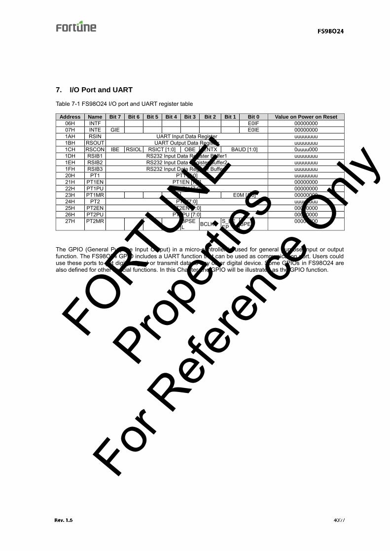
7. I/O PORT AND UART ............................................................................................................................... 40
13. CPU RESET ............................................................................................................................................. 61
14. HALT AND SLEEP MODES ..................................................................................................................... 63
15. INSTRUCTION SET ................................................................................................................................. 64
15.1. Instruction Set Summary ............................................................................................................ 64
17. REVISION HISTORY ................................................................................................. 錯誤! 尚未定義書籤。
FORTU
NE'
Propert
ies
For R
eferen
ce O
nly
Figure List
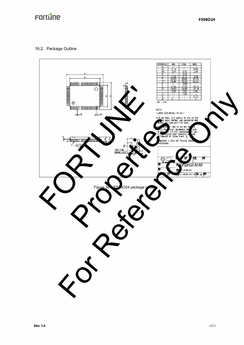
Figure 1-1 FS98O24 pin configuration ......................................................................................... 10 Figure 1-2 FS98O24 function block .............................................................................................. 13 Figure 1-3 FSC 8-bit CPU core function block ............................................................................. 14 Figure 1-4 FSC CPU instruction cycle .......................................................................................... 15 Figure 2-1 VDDA vs Temp @ VDD=3V …………………………………………………………………..17 Figure 2-2 VREF vs Temp @ VDD=3V ........................................................................................... 17 Figure 3-1 FS98O24 program memory structure ......................................................................... 18 Figure 3-2 IND & FSR function description .................................................................................. 20 Figure 4-1 FS98O24 power system block .................................................................................... 25 Figure 4-2 Voltage Doubler ............................................................................................................ 28 Figure 4-3 Voltage regulator .......................................................................................................... 29 Figure 4-4 analog bias circuit ....................................................................................................... 30 Figure 4-5 analog common voltage generator ............................................................................. 31 Figure 4-6 low battery comparator function block ...................................................................... 32 Figure 4-7 Bandgap voltage and temperature sensor function block ....................................... 33 Figure 5-1 FS98O24 oscillator state block ................................................................................... 34 Figure 6-1 Dual 24-bit programmable counter functional block ................................................ 36 Figure 6-2 FS98O24 timer module function block ....................................................................... 38 Figure 6-3 watch dog timer function block .................................................................................. 39 Figure 6-4 Programmable Counter Working block diagram ....................................................... 39 Figure 7-1 FS98O24 GPIO port 1 functional block ...................................................................... 41 Figure 7-2 FS98O24 GPIO port 2 functional block ...................................................................... 42 Figure 8-1 FS98O24 DMM network function block ...................................................................... 44 Figure 8-2 FS98O24 ADC function block ...................................................................................... 46 Figure 10-1 The FS98O24 OPAMP functional block .................................................................... 50 Figure 10-2 single end amplifier application example ................................................................ 52 Figure 10-3 differential amplifier example ................................................................................... 52 Figure 11-1 Comparator functional block..................................................................................... 53 Figure 12-1 LCD driver control block ........................................................................................... 56 Figure 16-1 FS98O24 package outline .......................................................................................... 76 Figure 16-2 FS98O24 package outline .......................................................................................... 77
FORTU
NE'
Propert
ies
For R
eferen
ce O
nly
Table List
Table 1-1 Ordering Information ....................................................................................................... 9 Table 1-2 FS98O24 pin description ................................................................................................ 11 Table 2-1 FS98O24 absolute maximum rating table .................................................................... 16 Table 2-2 FS98O24 DC characteristics ......................................................................................... 16 Table 2-3 FS98O24 ADC characteristics ....................................................................................... 17 Table 2-4 FS98O24 OPAMP characteristics ................................................................................. 17 Table 3-1 FS98O24 Data memory structure ................................................................................. 18 Table 3-2 system register table ..................................................................................................... 19 Table 3-3 A table of WDT reset differs to Ext. reset. .................................................................... 19 Table 3-4 peripheral special registers table ................................................................................. 24 Table 4-1 FS98O24 power system register table ......................................................................... 26 Table 4-2 Voltage Doubler register table ...................................................................................... 28 Table 4-3 Voltage Doubler operation frequency selection table ................................................. 29 Table 4-4 voltage regulator register table .................................................................................... 29 Table 4-5 analog bias circuit register table .................................................................................. 30 Table 4-6 analog common voltage generator register table ....................................................... 31 Table 4-7 low battery comparator register table .......................................................................... 32 Table 4-8 low battery comparator voltage detection selection table ......................................... 32 Table 4-9 bandgap voltage and temperature sensor register table ........................................... 33 Table 5-1 FS98O24 clock system register table ........................................................................... 34 Table 5-2 MCK selection table ....................................................................................................... 34 Table 5-3 FS98O24 CPU instruction cycle register table ............................................................ 35 Table 5-4 instruction cycle selection table ................................................................................... 35 Table 5-5 beeper clock register table............................................................................................ 35 Table 6-1 Programmable counter module register table ............................................................. 36 Table 6-2 Timer module register table .......................................................................................... 38 Table 6-3 watch dog timer register table ...................................................................................... 38 Table 7-1 FS98O24 I/O port and UART register table .................................................................. 40 Table 7-2 FS98O24 I/O port and UART register table .................................................................. 41 Table 7-3 FS98O24 I/O port and UART register table .................................................................. 42 Table 8-1 DMM function network register table ........................................................................... 45 Table 8-2 ADC function register table ........................................................................................... 47 Table 9-1 ADC rolling counts versus ADM ................................................................................... 49 Table 9-2 ADC rolling counts versus VR ...................................................................................... 49 Table 10-1 FS98O24 OPAMP control register table ..................................................................... 51 Table 11-1 FS98O24 comparator control register table ............................................................... 53 Table 12-1 FS98O24 LCD driver register table ............................................................................. 56 Table 13-1 FS98O24 initial status table ........................................................................................ 61 Table 15-1 FS98O24 instruction set table ..................................................................................... 64
FORTU
NE'
Propert
ies
For R
eferen
ce O
nly
1. Device Overview
The FS98O24 is an 8-bit RISC-like microcontroller with 4k x 16 bits OTP program memory, auto range DMM function network, one 14-bit fully differential input analog to digital converter, two low noise amplifiers, and 4 COM x 20 SEG LCD driver. The FS98O24 is best suitable for applications such as 3 3/4 DMM and other measurement instrument products.
1.1. High Performance RISC CPU An 8-bit microcontroller with 37 single word instructions. Embedded 4k x 16 bits One-Time-Programmable(OTP) program memory. 256-byte data memory (SRAM). 8-level deep stacks.
1.2. Peripheral Features Embedded internal oscillator. External 32768Hz (RTC) or 4MHz crystal oscillator. Embedded Low Voltage Reset (LVR) and Low Voltage Detector (LVD) [3 mode: <2.3V, <3.5V, ADP2]. Dual 24-bit Programmable counter. 8-bit Frequency Synthesizer. 16-bit bi-directional I/O port. Buzzer output. 4 x 20 LCD drivers. UART. Two low noise amplifier One 14-bit fully differential input analog to digital converter(ADC) Auto range DMM function network can measure:
1.3. Analog Features One 14-bit ADC with programmable output rate and resolution (10-bit/320Hz~14-bit/5Hz). Two low noise (1μV Vpp without chopper, 0.5μV Vpp with chopper, 0.1Hz~1Hz) OPAMP with chopper
controller.
1.4. Special Microcontroller Features Embedded 580KHz oscillator. External 32768Hz (RTC) or 4MHz crystal oscillator. Embedded Low Voltage Reset (LVR) and Low Voltage Detector (LVD) [3 mode: <2.3V, <3.3V, ADP2]. 7 Interrupt sources (external: 3, internal: 4). Embedded charge pump (Voltage Doubler) and voltage regulator (3.6V regulated output).
FORTU
NE'
Propert
ies
For R
eferen
ce O
nly
Embedded bandgap voltage reference (typical 1.16V±50mV, 100ppm/°C). Internal silicon temperature sensor (typical 550μV50μV/C). Watchdog timer (WDT). Package: 100-pin QFP.
1.5. CMOS Technology Voltage operation range from 2.2V to 5.0V. Operation current is less than 4 mA; power down mode current is about 3μA.
1.6. Applications 3 3/4 auto-range DMM. Measurement instrument. Digital meter.
1.7. Ordering Information
Table 1-1 Ordering Information
Product Number Description Package Type
FS98O24-PEF MCU with OTP ROM; The customer has to program the compiled hex code into OTP ROM.
100-pin QFP
FS98O24-nnn-PEF MCU with program type; FSC programs the customer’s compiled hex code into OTP ROM at factory before shipping.
100-pin QFP
FS98O24-D MCU with OTP ROM; The customer has to program the compiled hex code into OTP ROM.
Dice form
FS98O24-nnn-D MCU with program type; FSC programs the customer’s compiled hex code into OTP ROM at factory before shipping.
Dice form
Note1: Code number (nnn) is assigned for customer.
Note2: Code number (nnn = 001~999).
FORTU
NE'
Propert
ies
For R
eferen
ce O
nly
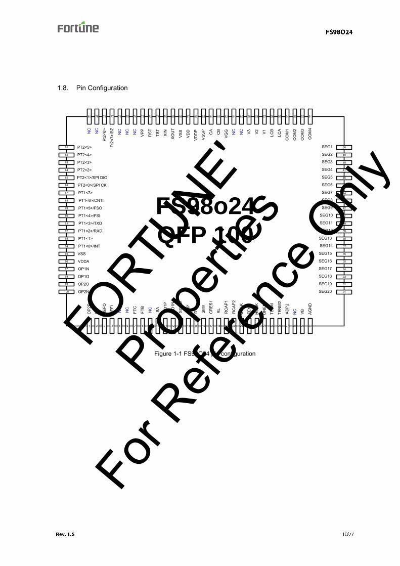
1.8. Pin Configuration
FS98o24
QFP 100
1
NC
2
REF
O
3
REF
I
4
NC
5
NC
6
FTC
7
FTB
8
NC
9 10
RL
11
RC
AP1
12
RC
AP2
13
ON
EK
14
TEN
K
15
HU
NK
16
ON
EM
17
TEN
M
18
TEN
M2
19 20 21
ADP2
22
NC
23
VB
24
AGN
D
25 26 27 28 29 30
80N
C79 78 77
PT2<4>
76
NC
75
NC
74 73
Pt2<
6>
72
Pt2<
7>/B
Z53
NC
52
NC
71
VPP
70
RST
69
TST
68 67
XIN
66
XOU
T
65
VSS
64
VDD
63
VDD
P
62
VSSP
61
CA
60
CB
59
VGG
58
NC
57
NC
56
V3
55 54 51
81
82
PT2<3>83
PT2<2>84
PT2<1>/SPI DIO85
PT2<0>/SPI CK86
PT1<7>87
PT1<4>/FSI90
PT1<3>/TXD91
PT1<2>/RXD92
PT1<1>93
PT1<0>/INT94
OP1N97
OP1O98
OP2O99
OP2N100
SEG4
SEG5
49
SEG6
48
SEG7
47
SEG8
46
SEG9
45
SEG10
44
SEG11
43
SEG12
42
SEG15
41
SEG16
40
39
38
SEG17
37
SEG18
35
35
34
33
32
31
OP2
P
SEG3
SEG1
SEG2SA AD
1P
AD1N
SGN
D
ADP
DT SM
V
CR
ES1
V2 V1 LCB
LCA
CO
M1
CO
M2
CO
M3
CO
M4
VSS95
VDDA96
PT1<6>/CNTI88
PT1<5>/FSO89
PT2<5>
SEG20
SEG19
SEG14
SEG13
50
Figure 1-1 FS98O24 pin configuration
FORTU
NE'
Propert
ies
For R
eferen
ce O
nly
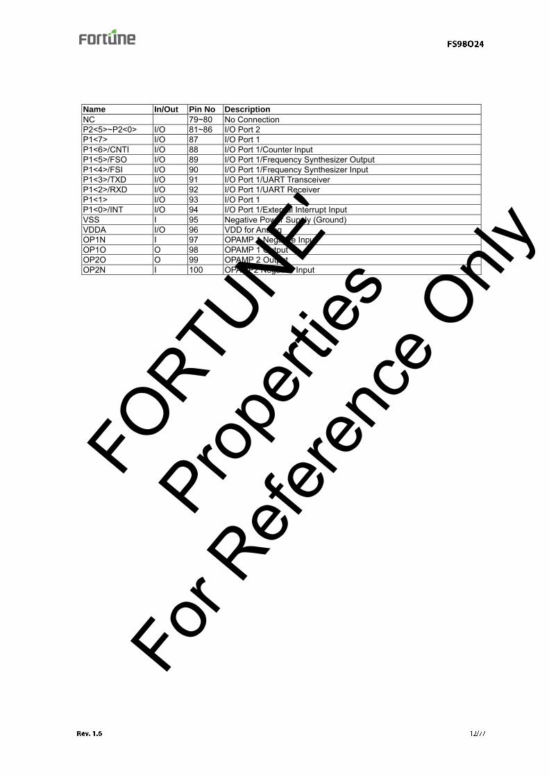
1.9. Pin Description
Table 1-2 FS98O24 pin description
Name In/Out Pin No Description
OP2P I 1 OPAMP 2 Positive Input NC 2 No Connection REFO O 3 Band gap Reference Output REFI I 4 ADC Reference Voltage Input NC 5,6 NC Connection FTC, FTB I/O 7,8 ADC Pre-Filter Capacitor Connection NC 9 No Connection SA I 10 ADC Input of Current measurement AD1P I 11 ADC Positive input of AC measurement AD1N I 12 ADC Negative input of AC measurement SGND I 13 Sensing point for analog ground ADP I 14 ADC Input DT I 15 Diode measurement Voltage Divide Resistance Sensing point SMV I 16 High impedance input terminal (DCmV Terminal) CRES1 I 17 The terminal of filter capacitor under resistance measurement RL I 18 Negative input of ADC reference under resistance measurement RCAP1 O 19 Capacitance measurement voltage source RCAP2 O 20 Capacitance measurement voltage source ONEK I 21 Voltage/Resistance measurement attenuator (1.000kΩ) TENK I 22 Voltage/Resistance measurement attenuator (10.01kΩ) HUNK I 23 Voltage/Resistance measurement attenuator (100.1kΩ) ONEM I 24 Voltage/Resistance measurement attenuator (1.111MΩ) TENM I 25 Voltage/Resistance measurement attenuator (10MΩ) TENM2 I 26 Voltage/Resistance measurement attenuator (10MΩ) ADP2 I 27 Extra ADC Input NC 28 No Connection VB I 29 Analog Circuit Bias Current Input AGND I/O 30 Analog Ground SEG20~SEG1 O 31~50 LCD Segment Driver Output COM4~COM1 O 51~54 LCD Common Driver Output LCA I/O 55 LCD Charge Pump Capacitor Positive Connection LCB I/O 56 LCD Charge Pump Capacitor Negative Connection V1,V2,V3 I/O 57~59 LCD Bias NC 60 No Connection NC 61 No Connection VGG I/O 62 Charge Pump Voltage CB I/O 63 Charge Pump Capacitor Positive Connection CA I/O 64 Charge Pump Capacitor Negative Connection VSSP I 65 Charge Pump Negative Power Supply VDDP I 66 Charge Pump Positive Power Supply
VDD I 67 Positive Power Supply VSS I 68 Negative Power Supply (Ground) XOUT O 69 32768Hz/4MHz Oscillator Output XIN I 70 32768Hz/4MHz Oscillator Input TST I 71 Testing Mode RST I 72 CPU Reset VPP I 73 Programming Power Supply NC 74~76 No Connection P2<7>/BZ I/O 77 I/O Port 2/Buzzer Output P2<6> I/O 78 I/O Port 2
FORTU
NE'
Propert
ies
For R
eferen
ce O
nly
Name In/Out Pin No Description
NC 79~80 No Connection P2<5>~P2<0> I/O 81~86 I/O Port 2 P1<7> I/O 87 I/O Port 1 P1<6>/CNTI I/O 88 I/O Port 1/Counter Input P1<5>/FSO I/O 89 I/O Port 1/Frequency Synthesizer Output P1<4>/FSI I/O 90 I/O Port 1/Frequency Synthesizer Input P1<3>/TXD I/O 91 I/O Port 1/UART Transceiver P1<2>/RXD I/O 92 I/O Port 1/UART Receiver P1<1> I/O 93 I/O Port 1 P1<0>/INT I/O 94 I/O Port 1/External Interrupt Input VSS I 95 Negative Power Supply (Ground) VDDA I/O 96 VDD for Analog OP1N I 97 OPAMP 1 Negative Input OP1O O 98 OPAMP 1 Output OP2O O 99 OPAMP 2 Output OP2N I 100 OPAMP2 Negative Input
FORTU
NE'
Propert
ies
For R
eferen
ce O
nly
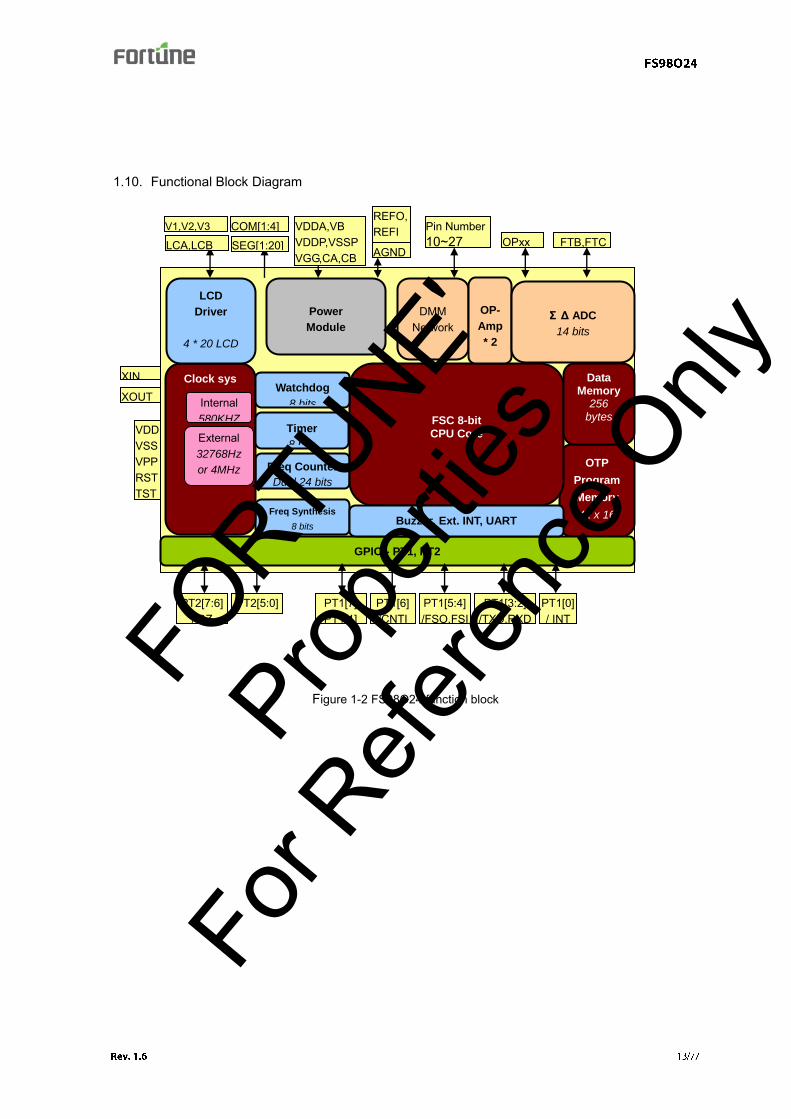
1.10. Functional Block Diagram
Figure 1-2 FS98O24 function block
Freq Synthesis
8 bits
Freq Counter
Dual 24 bits
OTP
Program
Memory
4k x 16
bits
REFO, REFI
DMM
Network
FSC 8-bit CPU Core
Data Memory
256 bytes
Clock sys
Internal 580KHZ
External 32768Hz
or 4MHz
LCD
Driver
4 * 20 LCD
Timer
8 bits
OP-
Amp
* 2
Σ Δ ADC
14 bits
Power
Module
FTB,FTC AGND SEG[1:20]
COM[1:4] LCA,LCB V1,V2,V3
GPIO - PT1, PT2
Buzzer, Ext. INT, UART
PT1[3:2] /TXD,RXD
PT1[5:4] /FSO,FSI
PT1[6] /CNTI
PT2[7:6] / BZ
Watchdog
8 bits
OPxx
PT1[0] / INT
VDDA,VB VDDP,VSSP VGG,CA,CB
PT2[5:0] PT1[7] PT1[1]
Pin Number 10~27
VDD VSS VPP RST TST
XOUT XIN
FORTU
NE'
Propert
ies
For R
eferen
ce O
nly
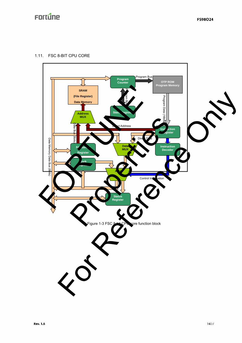
1.11. FSC 8-BIT CPU CORE
Figure 1-3 FSC 8-bit CPU core function block
Stack Register
OTP ROM
Program Memory
Program
Counter
Instruction Register
Address
MUX
File Select
Register
(FSR)
SRAM
(File Register)
Data Memory
Instruction Decoder
Data MUX
ALU
Work
Register
Status Register
Control Information
Direct Address
Direct Data
Program D
ata (16bits)
Data M
emory D
ata Bus (8bits)
Program Bus
Program Bus
Data Bus (8bits)
FORTU
NE'
Propert
ies
For R
eferen
ce O
nly
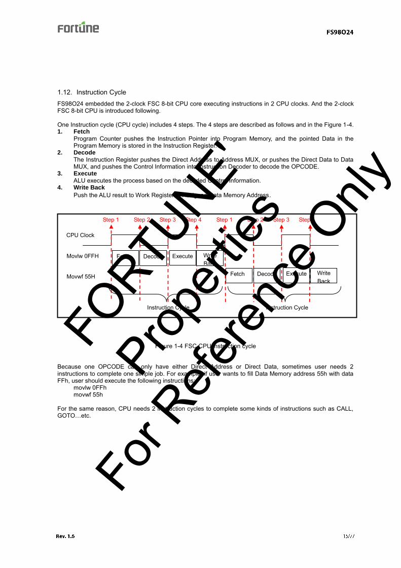
1.12. Instruction Cycle FS98O24 embedded the 2-clock FSC 8-bit CPU core executing instructions in 2 CPU clocks. And the 2-clock FSC 8-bit CPU is introduced following. One Instruction cycle (CPU cycle) includes 4 steps. The 4 steps are described as follows and in the Figure 1-4. 1. Fetch
Program Counter pushes the Instruction Pointer into Program Memory, and the pointed Data in the Program Memory is stored in the Instruction Register.
2. Decode
The Instruction Register pushes the Direct Address to Address MUX, or pushes the Direct Data to Data MUX, and pushes the Control Information into Instruction Decoder to decode the OPCODE.
3. Execute
ALU executes the process based on the decoded Control Information. 4. Write Back
Push the ALU result to Work Register or Assigned Data Memory Address.
Figure 1-4 FSC CPU instruction cycle
Because one OPCODE can only have either Direct Address or Direct Data, sometimes user needs 2 instructions to complete one simple job. For example, if user wants to fill Data Memory address 55h with data FFh, user should execute the following instructions:
movlw 0FFh movwf 55h
For the same reason, CPU needs 2 instruction cycles to complete some kinds of instructions such as CALL, GOTO…etc.
Supply Voltage on VDD 3.6 V Input Voltage on any pin -0.3 to VDD+0.3 V Ambient Operating Temperature -40* to +85 C Storage Temperature -55 to +150 C Soldering Temperature, Time 260C, 10 Sec * FS98O24 passed -40C LTOL (Low Temperature Operating Life) test (VDD=3V)
2.2. DC Characteristics (VDD=3V, TA=25℃, unless otherwise noted)
Table 2-2 FS98O24 DC characteristics
Symbol Parameter Test Condition Min. Typ. Max. Unit
VDD Recommend Operation Power Voltage 2.2 5.0 V VDDP Charge pump Power Voltage ENPUMP=1 2.2 3.6 V IDD Supply Current CPU, ADC On 4 mA IPO Power-off Supply Current At Power Off 3 μA VIH Digital Input High Voltage PT1, Reset 0.7 VDD VIL Digital Input Low Voltage PT1, Reset 0.3 VDD VIHSH Input hysteresis High Voltage Schmitt-trigger port 0.45 VDD VIHSL Input hysteresis Low Voltage Schmitt-trigger port 0.20 VDD IPU Pull up Current Vin=0 20 μA IOH High Level Output Current VOH=VDD-0.3 V 3 mA IOL Low Level Output Current VOL=0.3 V 5 mA VDDA Analog Power 3.6 V
IREG VDDA Regulator Output Current VDD=3V,Internal Voltage Double, 0.95*VDDA
6 mA
VCVDDA VDDA Voltage Coefficient -2 2 %/V AGND Analog Ground Voltage VDD
A/2 V
ISI_AGND Analog Ground Sink Current 1.05*AGND 1 mA ISO_AGND Analog Ground Source Current 0.95*AGND 1 mA VREF Build in Reference Voltage REFO To AGND 1.16 V VCREF Build in Reference Voltage Supply Voltage
Coefficient -200
0 +200
0 ppm/V
TCREF Build in Reference Voltage Temperature Coefficient
Ta=0~50℃ 100 ppm/℃
TEMPH-TEMPL
Slope of {TEMPH-TEMPL} vs. Temperature 550 μV/C
VLBAT Low Battery Detector Voltage S_LB [1:0]=00 2.3 V S_LB [1:0]=01 3.5 V FLCD LCD Frame Frequency LCDCK[1:0]=10 32 Hz ICK Internal RC oscillator 530 670 800 KHz WDTCLK Internal WatchDog oscillator 1.7 KHz
Symbol Parameter Test Conditions Min. Typ. Max. Unit
VAIN ADC Common Mode Input Range INH,INL,VRH,VRL to VSS 0.6 0 2.3 V VRFIN ADC Differential Mode Input Range (INH,INL), (VRH,VRL) 0.6 V Resolution 15625 312501 Counts ADC Linearity Error VRFIN=0.44V -0.1 0 +0.1 mV
Symbol Parameter Test Conditions Min. Typ. Max. Unit
Input Offset 1.5 mV Input Offset Voltage with Chopper Rs<100Ω 20 μ V Input Reference Noise Rs=100Ω , 0.1Hz~1Hz 1.0 μ Vpp Input Reference Noise with Chopper Rs=100Ω , 0.1Hz~1Hz 0.5 μ Vpp Input Bias Current 10 30 pA Input Bias Current with Chopper 100 300 pA Input Common Mode Range 0.5 2.4 V Output Voltage Range 0.5 2.4 V Chopper Clock Frequency S_CHCK[1:0]=11 1k Hz Capacitor Load 50 100 pF
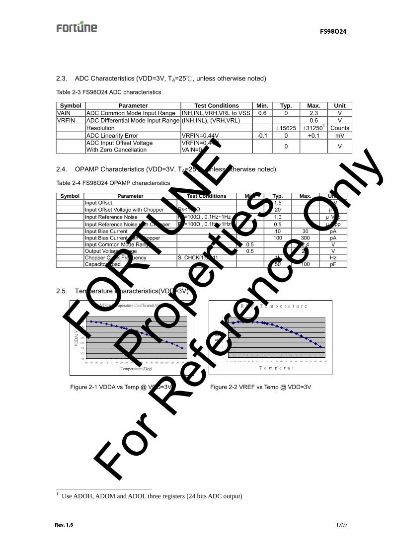
Figure 2-1 VDDA vs Temp @ VDD=3V Figure 2-2 VREF vs Temp @ VDD=3V
1 Use ADOH, ADOM and ADOL three registers (24 bits ADC output)
FORTU
NE'
Propert
ies
For R
eferen
ce O
nly
3. Memory Organization
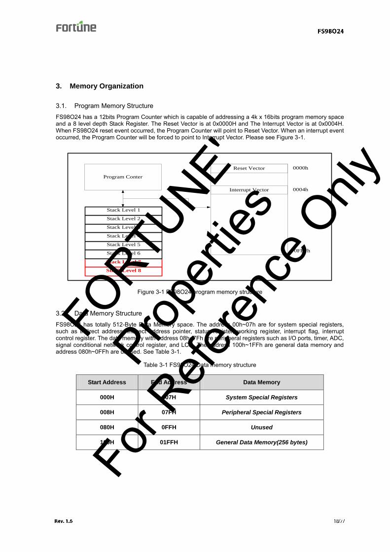
3.1. Program Memory Structure FS98O24 has a 12bits Program Counter which is capable of addressing a 4k x 16bits program memory space and a 8 level depth Stack Register. The Reset Vector is at 0x0000H and The Interrupt Vector is at 0x0004H. When FS98O24 reset event occurred, the Program Counter will point to Reset Vector. When an interrupt event occurred, the Program Counter will be forced to point to Interrupt Vector. Please see Figure 3-1.
Program Conter
Reset Vector
Interrupt Vector
0000h
0004h
0FFFh
Stack Level 7
Stack Level 8
Stack Level 6
Stack Level 5
Stack Level 3
Stack Level 4
Stack Level 2
Stack Level 1
Figure 3-1 FS98O24 program memory structure
3.2. Data Memory Structure FS98O24 has totally 512-Byte Data Memory space. The address 00h~07h are for system special registers, such as indirect address, indirect address pointer, status register, working register, interrupt flag, interrupt control register. The data memory with address 08h~7Fh are peripheral registers such as I/O ports, timer, ADC, signal conditional network control register, and LCD. The address 100h~1FFh are general data memory and address 080h~0FFh are unused. See Table 3-1.
Table 3-1 FS98O24 Data memory structure
Start Address End Address Data Memory
000H 007H System Special Registers
008H 07FH Peripheral Special Registers
080H 0FFH Unused
100H 01FFH General Data Memory(256 bytes)
FORTU
NE'
Propert
ies
For R
eferen
ce O
nly
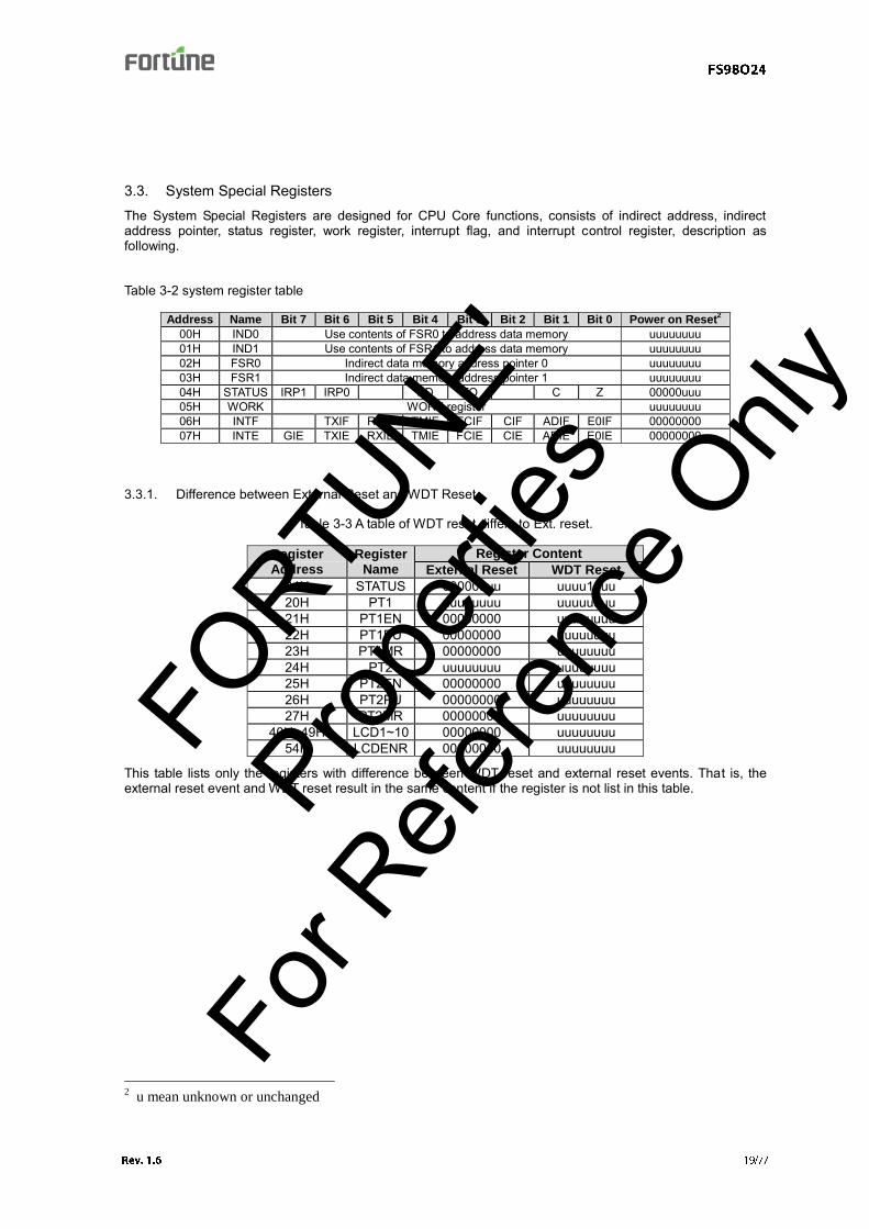
3.3. System Special Registers The System Special Registers are designed for CPU Core functions, consists of indirect address, indirect address pointer, status register, work register, interrupt flag, and interrupt control register, description as following.
Table 3-2 system register table
Address Name Bit 7 Bit 6 Bit 5 Bit 4 Bit 3 Bit 2 Bit 1 Bit 0 Power on Reset2
00H IND0 Use contents of FSR0 to address data memory uuuuuuuu 01H IND1 Use contents of FSR1 to address data memory uuuuuuuu 02H FSR0 Indirect data memory address pointer 0 uuuuuuuu 03H FSR1 Indirect data memory address pointer 1 uuuuuuuu 04H STATUS IRP1 IRP0 PD TO C Z 00000uuu 05H WORK WORK register uuuuuuuu 06H INTF TXIF RXIF TMIF FCIF CIF ADIF E0IF 00000000 07H INTE GIE TXIE RXIE TMIE FCIE CIE ADIE E0IE 00000000
3.3.1. Difference between External Reset and WDT Reset
Table 3-3 A table of WDT reset differs to Ext. reset.
This table lists only the registers with difference between WDT reset and external reset events. That is, the external reset event and WDT reset result in the same content if the register is not list in this table.
2 u mean unknown or unchanged
FORTU
NE'
Propert
ies
For R
eferen
ce O
nly
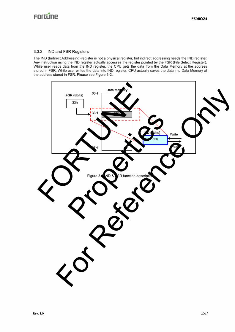
3.3.2. IND and FSR Registers The IND (Indirect Addressing) register is not a physical register, but indirect addressing needs the IND register. Any instruction using the IND register actually accesses the register pointed by the FSR (File Select Register). While user reads data from the IND register, the CPU gets the data from the Data Memory at the address stored in FSR. While user writes the data into IND register, CPU actually saves the data into Data Memory at the address stored in FSR. Please see Figure 3-2.
Figure 3-2 IND & FSR function description
Data Memory
00H
FFH
55h 33H
33h
FSR (8bits)
55h
IND (8bits) Write
Read
FORTU
NE'
Propert
ies
For R
eferen
ce O
nly
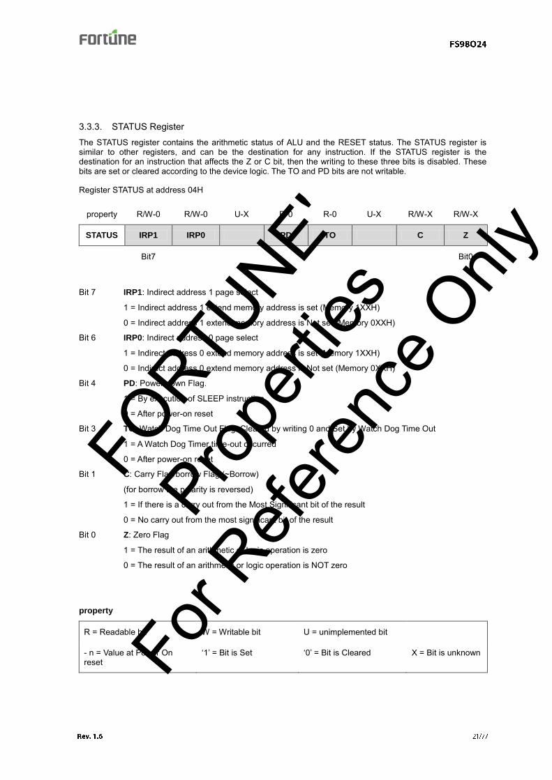
3.3.3. STATUS Register The STATUS register contains the arithmetic status of ALU and the RESET status. The STATUS register is similar to other registers, and can be the destination for any instruction. If the STATUS register is the destination for an instruction that affects the Z or C bit, then the writing to these three bits is disabled. These bits are set or cleared according to the device logic. The TO and PD bits are not writable.
Register STATUS at address 04H
property R/W-0 R/W-0 U-X R-0 R-0 U-X R/W-X R/W-X
STATUS IRP1 IRP0 PD TO C Z
Bit7 Bit0
Bit 7 IRP1: Indirect address 1 page select
1 = Indirect address 1 extend memory address is set (Memory 1XXH)
0 = Indirect address 1 extend memory address is Not set (Memory 0XXH)
Bit 6 IRP0: Indirect address 0 page select
1 = Indirect address 0 extend memory address is set (Memory 1XXH)
0 = Indirect address 0 extend memory address is Not set (Memory 0XXH)
Bit 4 PD: Power down Flag.
1 = By execution of SLEEP instruction
0 = After power-on reset
Bit 3 TO: Watch Dog Time Out Flag. Cleared by writing 0 and Set by Watch Dog Time Out
1 = A Watch Dog Timer time-out occurred
0 = After power-on reset
Bit 1 C: Carry Flag/borrow Flag (~Borrow)
(for borrow the polarity is reversed)
1 = If there is a carry out from the Most Significant bit of the result
0 = No carry out from the most significant bit of the result
Bit 0 Z: Zero Flag
1 = The result of an arithmetic or logic operation is zero
0 = The result of an arithmetic or logic operation is NOT zero
property
R = Readable bit W = Writable bit U = unimplemented bit
- n = Value at Power On reset
‘1’ = Bit is Set ‘0’ = Bit is Cleared X = Bit is unknown
FORTU
NE'
Propert
ies
For R
eferen
ce O
nly
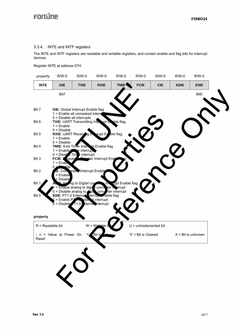
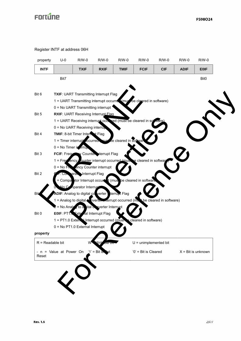
3.3.4. INTE and INTF registers The INTE and INTF registers are readable and writable registers, and contain enable and flag bits for interrupt devices.
1 = UART Transmitting interrupt occurred (must be cleared in software)
0 = No UART Transmitting interrupt
Bit 5 RXIF: UART Receiving Interrupt Flag
1 = UART Receiving interrupt occurred (must be cleared in software)
0 = No UART Receiving interrupt
Bit 4 TMIF: 8-bit Timer Interrupt Flag
1 = Timer interrupt occurred (must be cleared in software)
0 = No Timer interrupt
Bit 3 FCIF: Frequency Counter Interrupt Flag
1 = Frequency Counter interrupt occurred (must be cleared in software)
0 = No Frequency Counter interrupt
Bit 2 CIF: Comparator Interrupt Flag
1 = Comparator Interrupt occurred (must be cleared in software)
0 = No Comparator Interrupt
Bit 1 ADIF: Analog to digital converter Interrupt Flag
1 = Analog to digital converter Interrupt occurred (must be cleared in software)
0 = No Analog to digital converter Interrupt
Bit 0 E0IF: PT1.0 External Interrupt Flag
1 = PT1.0 External Interrupt occurred (must be cleared in software)
0 = No PT1.0 External Interrupt
property
R = Readable bit W = Writable bit U = unimplemented bit
- n = Value at Power On Reset
‘1’ = Bit is Set ‘0’ = Bit is Cleared X = Bit is unknown
FORTU
NE'
Propert
ies
For R
eferen
ce O
nly
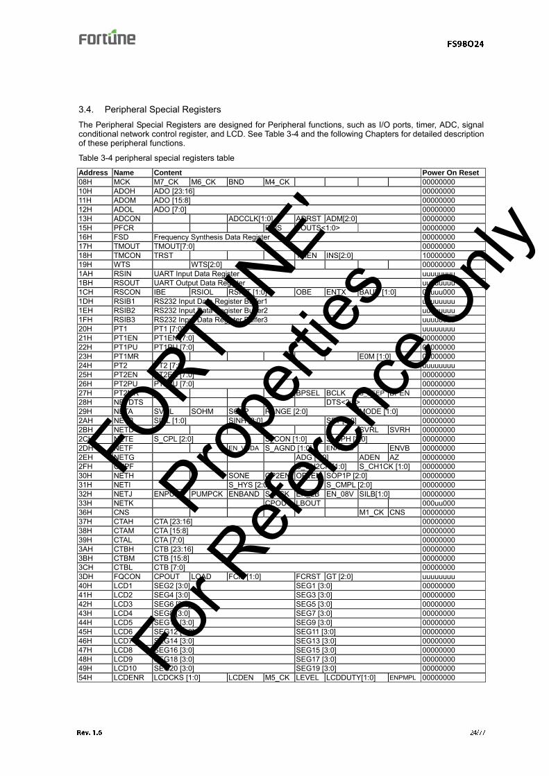
3.4. Peripheral Special Registers The Peripheral Special Registers are designed for Peripheral functions, such as I/O ports, timer, ADC, signal conditional network control register, and LCD. See Table 3-4 and the following Chapters for detailed description of these peripheral functions.
FS98O24 has a special power system supply whole chip work normally and only need two external capacitors. a fixed voltage (3.6V) for analog part. FS98O24 could work when the supply voltage is within a specified range, fixed or floating. The power system has six function engines includes Voltage Doubler, Voltage Regulator, Analog Circuit Bias Generator, Common Voltage Generator, Low Battery Detector and Band Gap Voltage Generator. Through the first 4 function engines, this system generates three voltage level and they are VGG = 2VDDP, VDDA = 3.6V, AGND = 1.8V. The voltage relationship is drawn in Figure 4-1. 1. Voltage Doubler
The acceptable VDDP range for FS98O24 is from 2.2V to 3.6V. Voltage Doubler raises the voltage of VGG to two times of VDDP3. VGG is used as the input of Voltage Regulator. It is from 4.4V to 7.2V. Please see Section 4.1 for detailed register setting.
2. Voltage Regulator
The fixed voltage value is important to analog function. Voltage Regulator raises the voltage of VDDA to fixed 3.6V. Although the input voltage of Voltage Regulator, VGG, is from 4.4V to 7.2V (It depends on the voltage of VDDP), the minimum possible voltage is still higher than 3.6V, so that Voltage Regulator could surely supply VDDA as 3.6V. Please refer to Section 4.2 for detailed register setting.
3. Analog Bias Circuit
Analog Bias Circuit is used for FS98O24 analog function. The user needs to enable Analog Bias Circuit, and then the Analog Functions such as ADC or OPAMP works correctly. Please refer to Section 4.3 for detailed register setting.
4. Common Voltage Generator
FS98O24 power system includes an analog ground generator. Please refer to Section 4.4 for detailed register setting.
Figure 4-1 FS98O24 power system block
3 VDDP means the VDD for Charge Pump (Voltage Doubler). User usually connects the VDDP to VDD.
VSSP means the VSS for Charge Pump (Voltage Doubler). User usually connects the VSSP to VSS.
VDDP
(2.2V~3.6V)
VSS / VSSP
(GND)
Voltage
Doubler
VGG = 2 VDDP
(4.4V~7.2V)
VDDA
(fixed 3.6V)
Voltage
Regulator
AGND = VDDA / 2
Common
Voltage
Generator
FORTU
NE'
Propert
ies
For R
eferen
ce O
nly
Table 4-1 FS98O24 power system register table Address Name Content
Bit 5 EN_VDDA: Voltage Regulator enable flag (Please refer to Section 4.5 for detailed description)
1 = Voltage Regulator is enabled, VDDA is 3.6V
0 = Voltage Regulator is disabled. VDDA can be from external power supply.
Bit 4-3 S_AGND[1:0]: Analog Common Voltage selector
11 = Analog Common Voltage is 2/3 VDDA. 10 = Analog Common Voltage is 1/3 VDDA. 01 = Analog Common Voltage is 1/2 VDDA. 00 = Analog Common Voltage is 1/4 VDDA.
Bit 2 ENAGND: Analog Common Voltage Generator enable flag
(Please see Section 4.4 for detailed description)
1 = Analog Common Voltage Generator is enabled. AGND voltage is selected by S_AGND[1:0].
0 = Analog Common Voltage Generator is disabled. AGND is floating.
Bit 0 ENVB: Analog Bias Circuit enable flag (Please see Section 4.3 for detailed description)
1 = Analog Bias Circuit is enabled. Analog system (ADC and OPAMP) can work correctly.
0 = Analog Bias Circuit is disabled. Analog system can NOT work
property
R = Readable bit W = Writable bit U = unimplemented bit
- n = Value at Power On Reset
‘1’ = Bit is Set ‘0’ = Bit is Cleared X = Bit is unknown
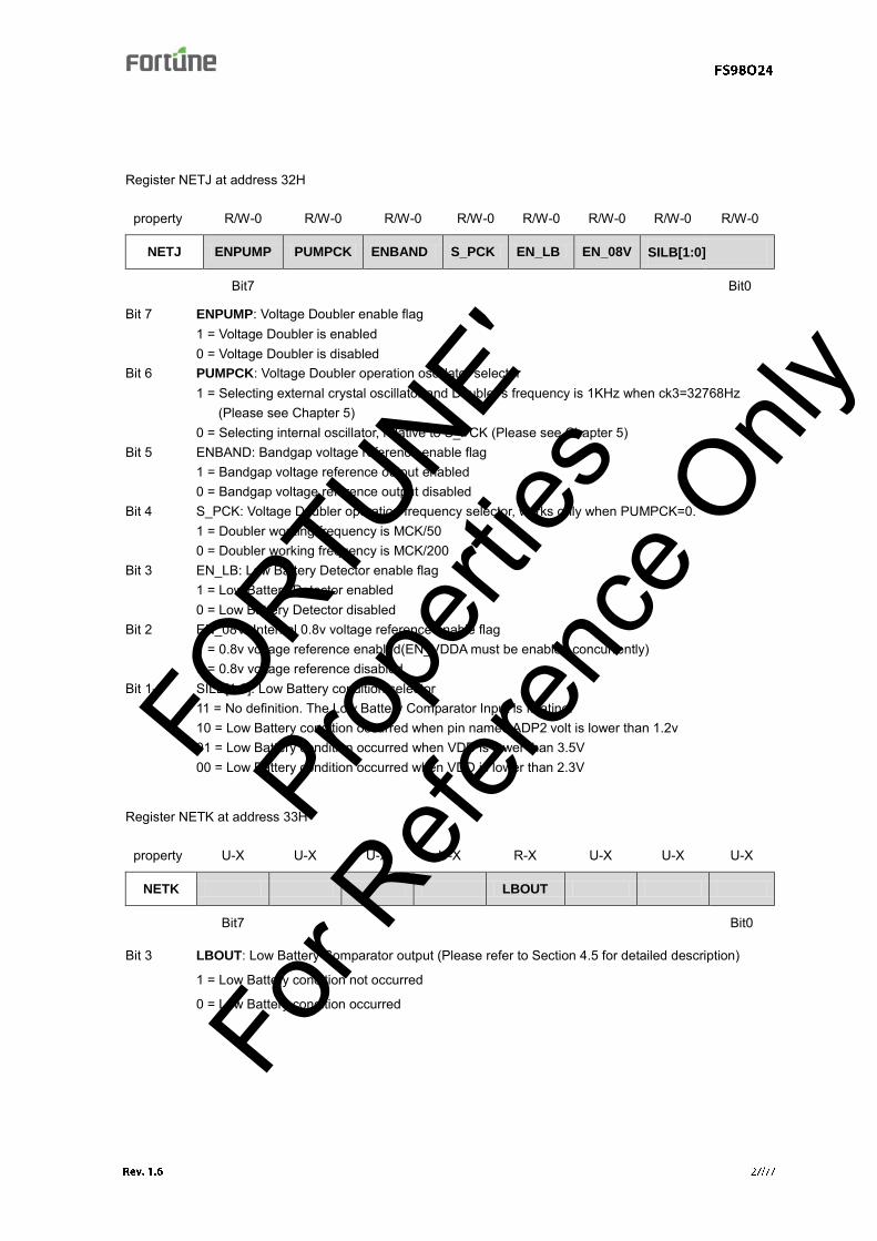
Bit 7 ENPUMP: Voltage Doubler enable flag 1 = Voltage Doubler is enabled 0 = Voltage Doubler is disabled Bit 6 PUMPCK: Voltage Doubler operation oscillator selector 1 = Selecting external crystal oscillator and Doubler’s frequency is 1KHz when ck3=32768Hz
(Please see Chapter 5) 0 = Selecting internal oscillator, relative to S_PCK (Please see Chapter 5) Bit 5 ENBAND: Bandgap voltage reference enable flag 1 = Bandgap voltage reference output enabled 0 = Bandgap voltage reference output disabled Bit 4 S_PCK: Voltage Doubler operation frequency selector, works only when PUMPCK=0. 1 = Doubler working frequency is MCK/50 0 = Doubler working frequency is MCK/200 Bit 3 EN_LB: Low Battery Detector enable flag 1 = Low Battery Detector enabled 0 = Low Battery Detector disabled Bit 2 EN_08V: Internal 0.8v voltage reference enable flag 1 = 0.8v voltage reference enabled(EN_VDDA must be enabled concurrently) 0 = 0.8v voltage reference disabled Bit 1-0 SILB[1:0]: Low Battery condition selector 11 = No definition. The Low Battery Comparator Input is floating. 10 = Low Battery condition occurred when pin named ADP2 volt is lower than 1.2v 01 = Low Battery condition occurred when VDD is lower than 3.5V 00 = Low Battery condition occurred when VDD is lower than 2.3V
Register NETK at address 33H
property U-X U-X U-X U-X R-X U-X U-X U-X
NETK LBOUT
Bit7 Bit0
Bit 3 LBOUT: Low Battery Comparator output (Please refer to Section 4.5 for detailed description)
1 = Low Battery condition not occurred
0 = Low Battery condition occurred
FORTU
NE'
Propert
ies
For R
eferen
ce O
nly
4.1. Voltage Doubler
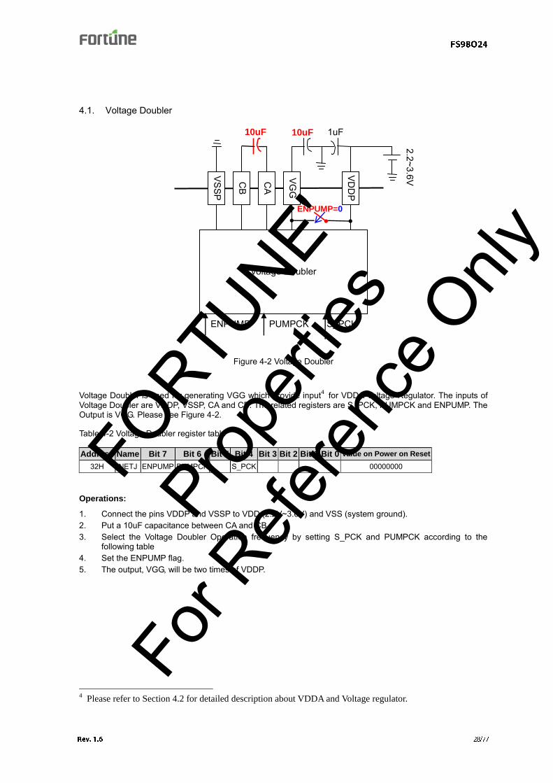
Figure 4-2 Voltage Doubler
Voltage Doubler is used for generating VGG which provide input4 for VDDA Voltage Regulator. The inputs of Voltage Doubler are VDDP, VSSP, CA and CB. The related registers are S_PCK, PUMPCK and ENPUMP. The Output is VGG. Please see Figure 4-2.
Table 4-2 Voltage Doubler register table
Address Name Bit 7 Bit 6 Bit 5 Bit 4 Bit 3 Bit 2 Bit 1 Bit 0 Value on Power on Reset
32H NETJ ENPUMP PUMPCK S_PCK 00000000
Operations:
1. Connect the pins VDDP and VSSP to VDD (2.2V~3.6V) and VSS (system ground). 2. Put a 10uF capacitance between CA and CB. 3. Select the Voltage Doubler Operation frequency by setting S_PCK and PUMPCK according to the
following table 4. Set the ENPUMP flag. 5. The output, VGG, will be two times of VDDP.
4 Please refer to Section 4.2 for detailed description about VDDA and Voltage regulator.
Voltage Doubler
VSSP
CB
CA
VGG
VDD
P
ENPUMP S_PCK
2.2~3.6V 10uF 1uF
PUMPCK
10uF
ENPUMP=0
FORTU
NE'
Propert
ies
For R
eferen
ce O
nly
Table 4-3 Voltage Doubler operation frequency selection table
PUMPCK S_PCK Voltage Doubler Operation Frequency
0 1 MCK/50 0 0 MCK/200 1 X CK3/32
If the user doesn’t want the VGG to be generated from the Voltage Doubler, then the ENPUMP should be set to disable the voltage Doubler, and input the VGG pin a voltage as voltage regulator power supply.
4.2. Voltage Regulator
Voltage Regulator
VG
G
VD
DA
C2 1uF
EN_VDDA
EN_VDDA
EN_08V
REFO08
Figure 4-3 Voltage regulator
Voltage Regulator is used for generating VDDA (3.6V). The input is VGG which is generated by Voltage Doubler (please see the Section 4.1). Please see Figure 4-3.
Table 4-4 voltage regulator register table
Address Name Bit 7 Bit 6 Bit 5 Bit 4 Bit 3 Bit 2 Bit 1 Bit 0 Value on Power on Reset
2DH NETF EN_VDDA 00000000
32H NETJ EN_08V 00000000
FORTU
NE'
Propert
ies
For R
eferen
ce O
nly
Operations
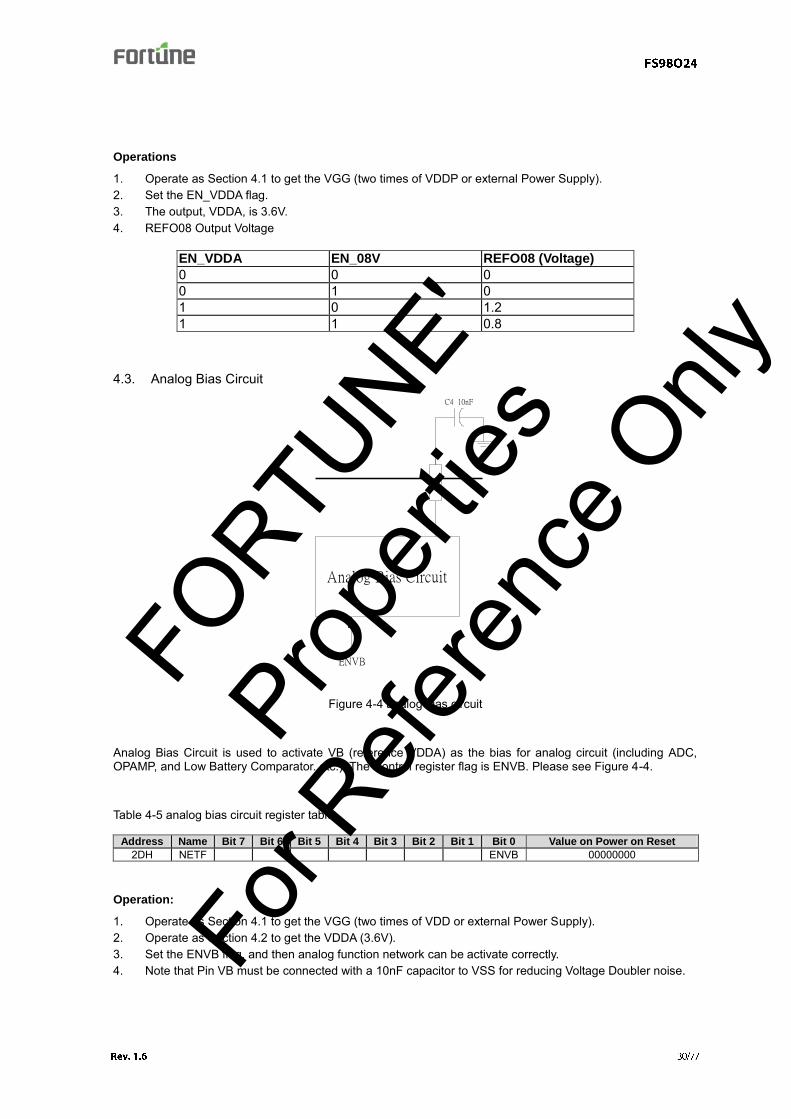
1. Operate as Section 4.1 to get the VGG (two times of VDDP or external Power Supply). 2. Set the EN_VDDA flag. 3. The output, VDDA, is 3.6V. 4. REFO08 Output Voltage
EN_VDDA EN_08V REFO08 (Voltage)
0 0 0 0 1 0 1 0 1.2 1 1 0.8
4.3. Analog Bias Circuit
Analog Bias Circuit
VB
C4 10nF
ENVB
Figure 4-4 analog bias circuit
Analog Bias Circuit is used to activate VB (reference VDDA) as the bias for analog circuit (including ADC, OPAMP, and Low Battery Comparator..etc.). The Control register flag is ENVB. Please see Figure 4-4.
Table 4-5 analog bias circuit register table
Address Name Bit 7 Bit 6 Bit 5 Bit 4 Bit 3 Bit 2 Bit 1 Bit 0 Value on Power on Reset
2DH NETF ENVB 00000000
Operation:
1. Operate as Section 4.1 to get the VGG (two times of VDD or external Power Supply). 2. Operate as Section 4.2 to get the VDDA (3.6V). 3. Set the ENVB flag, and then analog function network can be activate correctly. 4. Note that Pin VB must be connected with a 10nF capacitor to VSS for reducing Voltage Doubler noise.
FORTU
NE'
Propert
ies
For R
eferen
ce O
nly
4.4. Analog Common Voltage Generator
Analog Common Voltage Generator
AG
ND
C5 1uF
ENAGND S_AGND[1:0]
Figure 4-5 analog common voltage generator
Analog Common Voltage Generator is used to provide a common voltage for analog circuits. The Control registers are ENAGND and S_AGND[1:0] and the output is AGND. Please see Figure 4-5.
Table 4-6 analog common voltage generator register table
Address Name Bit 7 Bit 6 Bit 5 Bit 4 Bit 3 Bit 2 Bit 1 Bit 0 Value on Power on Reset
2DH NETF S_AGND [1:0] ENAGND 00000000
Operation:
1. Operate following the steps Chapter 4.1 to get the VGG (two times VDD or external Power Supply). 2. Operate as Section 4.2 to get the VDDA (3.6V) 3. Operate as Section 4.3 to activate the Analog Bias Circuit 4. Set the ENAGND to enable AGND generator. 5. Set the S_AGND[1:0] registers to select AGND output voltage, as the following:
S_AGND [1:0] AGND Voltage
00 1/4 VDDA 01 1/2 VDDA 10 1/3 VDDA 11 2/3 VDDA
FORTU
NE'
Propert
ies
For R
eferen
ce O
nly
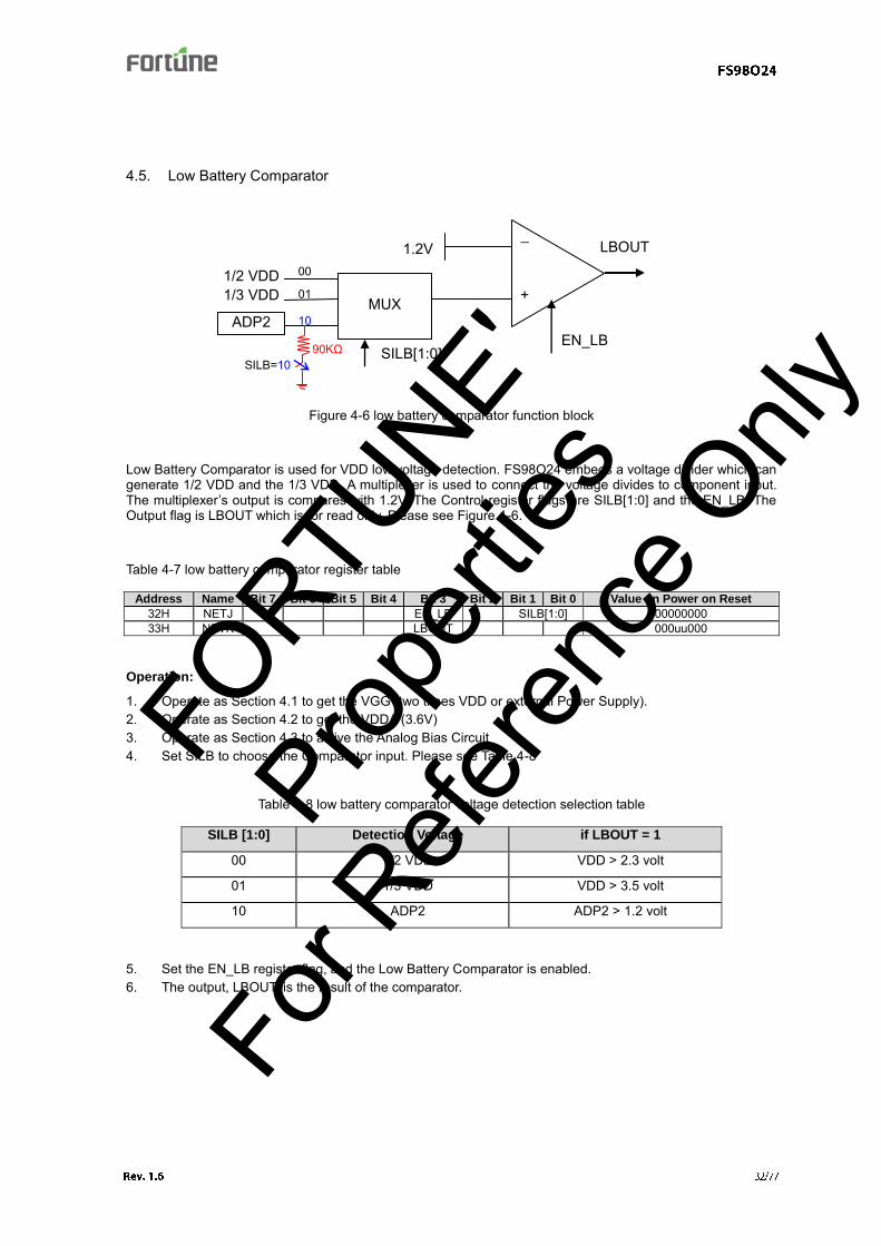
4.5. Low Battery Comparator
Figure 4-6 low battery comparator function block
Low Battery Comparator is used for VDD low voltage detection. FS98O24 embeds a voltage divider which can generate 1/2 VDD and the 1/3 VDD. A multiplexer is used to connect the voltage divides to component input. The multiplexer’s output is compares with 1.2V. The Control register flags are SILB[1:0] and the EN_LB. The Output flag is LBOUT which is for read only. Please see Figure 4-6.
Table 4-7 low battery comparator register table
Address Name Bit 7 Bit 6 Bit 5 Bit 4 Bit 3 Bit 2 Bit 1 Bit 0 Value on Power on Reset
1. Operate as Section 4.1 to get the VGG (two times VDD or external Power Supply). 2. Operate as Section 4.2 to get the VDDA (3.6V) 3. Operate as Section 4.3 to active the Analog Bias Circuit 4. Set SILB to choose the Comparator input. Please see Table 4-8
Table 4-8 low battery comparator voltage detection selection table
SILB [1:0] Detection Voltage if LBOUT = 1
00 1/2 VDD VDD > 2.3 volt
01 1/3 VDD VDD > 3.5 volt
10 ADP2 ADP2 > 1.2 volt
5. Set the EN_LB register flag, and the Low Battery Comparator is enabled. 6. The output, LBOUT, is the result of the comparator.
MUX
EN_LB
1.2V
1/2 VDD 1/3 VDD
SILB[1:0]
00
01
ADP2 10
+
_ LBOUT
90KΩ SILB=10
FORTU
NE'
Propert
ies
For R
eferen
ce O
nly
4.6. Bandgap Voltage and Temperature Sensor
Bandgap Voltage Referenceand Temperature Sensor
TEMPH
TEMPL
To Function Network
RE
FO
ENBAND
Figure 4-7 Bandgap voltage and temperature sensor function block
REFO is low temperature coefficient bandgap voltage reference output. Its voltage to AGND is 1.16V, and the typical temperature coefficient is 150ppm/C.
FS98O24 embeds a Temperature Sensor to measure the IC temperature from the differential voltage between TEMPH and TEMPL (typically 550μV50μV/C). Its working range is 100 ~ 200 mV. User can connect the TEMPH and TEMPL to an ADC to get the IC temperature.
Both the Bandgap Voltage Reference and the Temperature sensor are controlled by ENBAND register flag.
Please see Figure 4-7.
Table 4-9 bandgap voltage and temperature sensor register table
Address Name Bit 7 Bit 6 Bit 5 Bit 4 Bit 3 Bit 2 Bit 1 Bit 0 Value on Power on Reset
1DH NETJ ENBAND 00000000
Operation:
1. Operate as Section 4.1 to get the VGG (two times VDD or external Power Supply). 2. Operate as Section 4.2 to get the VDDA (3.6V) 3. Operate as Section 4.3 to enable the Analog Bias Circuit 4. Set the ENBAND register flag. 5. Check REFO. Its value with respect to AGND should be about 1.16V 6. The output, TEMPH and TEMPL, will show the IC temperature as the differential voltage.
FORTU
NE'
Propert
ies
For R
eferen
ce O
nly
5. Clock System
The clock system provides clock signals for the whole chip. The detailed setup will be illustrated in this chapter.
5.1. Oscillator States
580KHz Internal
Oscillator Circuit
32.768kHz/4MH
z Crystal
Oscillator CircuitX
IN
XO
UT
10M/1M
32.768kHz/4
MHz
CK2
CK3MCK
MUX2
25pF 25pF
BND
M4_CK
/ 2
Figure 5-1 FS98O24 oscillator state block
Table 5-1 FS98O24 clock system register table
Address Name Bit 7 Bit 6 Bit 5 Bit 4 Bit 3 Bit 2 Bit 1 Bit 0 Value on Power on Reset
08H MCK M7_CK M6_CK BND M4_CK 00000000 The internal and external oscillators are controlled by M7_CK and M6_CK, as shown in Table 5-2. External crystal oscillator can use 32768Hz(R=10MΩ)or 4MHz(R=1MΩ), register option:
When BND =0 then CK3 = 4MHz, when BND=1 then CK3=32768Hz. System operation frequency set by M4_CK5
. M4_CK=”0”, MCK=CK2; M4_CK=”1”, MCK=CK3/2. If users execute the sleep instruction to make FS98O24 enter the SLEEP mode, both the internal and
5 Users must make sure that switching from one oscillator to the other can be made only after the oscillator ’s
output is stabilized. And an NOP command should be added after the switching.
FORTU
NE'
Propert
ies
For R
eferen
ce O
nly
5.2. CPU Instruction Cycle
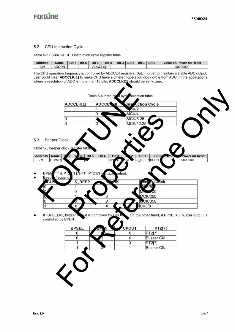
Table 5-3 FS98O24 CPU instruction cycle register table
Address Name Bit 7 Bit 6 Bit 5 Bit 4 Bit 3 Bit 2 Bit 1 Bit 0 Value on Power on Reset
13H ADCON ADCCLK[1:0] 00000000
The CPU operation frequency is controlled by ADCCLK registers. But, in order to maintain a stable ADC output, user could clear ADCCLK[1] to make CPU have a different operation clock cycle from ADC. In the applications where a resolution of ADC is more than 13 bits, ADCCLK[1] should be set to zero.
Table 5-4 instruction cycle selection table
ADCCLK[1] ADCCLK[0] Instruction Cycle
1 1 MCK/2 1 0 MCK/4 0 1 MCK/6.25 0 0 MCK/12.25
5.3. Beeper Clock
Table 5-5 beeper clock register table
Address Name Bit 7 Bit 6 Bit 5 Bit 4 Bit 3 Bit 2 Bit 1 Bit 0 Value on Power on Reset
27H PT2MR BPSEL BCLK S_BEEP BPEN 00000000
BPEN=”1” & PT2EN [7]=”1”: PT2 [7] is buzzer output. Beeper frequency :
BCLK S_BEEP M4_CK Beeper Clock
0 1 1 MCK/500 0 0 1 MCK/700 0 1 0 MCK/250 0 0 0 MCK/350 1 X X CK3/8
IF BPSEL=1, buzzer output is controlled by CPOUT. On the other hand, if BPSEL=0, buzzer output is
controlled by BPEN
BPSEL BPEN CPOUT PT2[7]
0 0 X PT2[7] 0 1 X Buzzer Clk 1 X 0 PT2[7] 1 X 1 Buzzer Clk
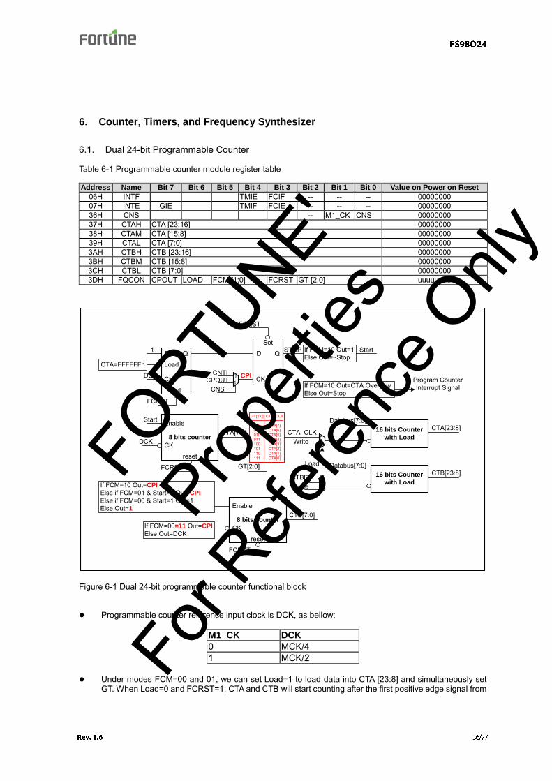
Programmable counter reference input clock is DCK, as bellow:
M1_CK DCK
0 MCK/4 1 MCK/2
Under modes FCM=00 and 01, we can set Load=1 to load data into CTA [23:8] and simultaneously set
GT. When Load=0 and FCRST=1, CTA and CTB will start counting after the first positive edge signal from
FORTU
NE'
Propert
ies
For R
eferen
ce O
nly
input CPI. The counters will not stop counting until CTA overflows and after the first positive edge signal from input CPI, and then the system will send out an interrupt signal. Therefore, we can count the cycles of CPI input signal to calculate the high-resolution frequency and duty cycle of the low frequency input signal by the following calculation approach.
Under mode FCM=10, CTA and CTB start counting when FCRST=1. The counters will not stop counting until CTA overflows, and then the system will send out an interrupt signal. The calculating flows and methods are described as follows:
Frequency Measurement Mode: FCM=00=11 (1) Load=1, FCRST=0. (2) Write to CTA [23:8] to set initial value of CTAI. (3) Set GT [2:0] to select the length of counter CTA. GT=000 sets CTA [23:8] as a 16-bit counter and
CTA [7] is as the clock input; CTA [23:0] is a 24-bit counter. GT=111 sets CTA [23:8] as a 16-bit counter and CTA [0] is as the clock input; {CTA [23:8], CTA [0]} is set as a 17-bit counter.
(4) Gate Time = (1000000h-CTAI x 256) x 1us … if GT=000. (5) Set LOAD=0, FCRST=1, and CPI frequency starts measuring. (6) Wait till positive edge of CPI, then Start=1 and CTA and CTB start counting. (7) Wait till CTA overflows and at the next positive edge of CPI, then Start=0 and CTA and CTB stop
counting. (8) When the CPU receives interrupt signal, the CPU will read CTA and CTB. Here CTA is the reference
clock counter, and CTB is the input clock counter.
(9) Frequency of CPI is
CTACTAI
CTBDCK . Go to (1) for next measurement.
Duty Cycle Measurement Mode: FCM=01
(1) Load=1, FCRST=0. (2) Write to CTA [23:8] to set initial value of CTAI. (3) Set GT [2:0] to select the length of counter CTA. GT=000 sets CTA [23:8] as a 16-bit counter and
CTA [7] is as the clock input; CTA [23:0] is a 24-bit counter. GT=111 sets CTA [23:8] as a 16-bit counter and CTA [0] is as the clock input; {CTA [23:8], CTA [0]} is set as a 17-bit counter.
(4) Gate Time = (1000000h-CTAI x 256) x 1us … if GT=000. (5) Set LOAD=0, FCRST=1, and CPI frequency starts measuring. (6) Wait till positive edge of CPI, then Start=1 and CTA and CTB start counting. (7) Wait till CTA overflows and at the next positive edge of CPI, then Start=0 and CTA and CTB stop
counting. (8) When the CPU receives interrupt signal, the CPU will read CTA and CTB. Here CTA is the reference
clock counter, and CTB is the input clock high pulse width counter.
(9) The duty cycle of CPI is
CTACTAI
CTB%100 . Go to (1) for next measurement.
Timer Mode: FCM=10
(1) Load=1, FCRST=0. (2) Write to CTA [23:8] to set initial value of CTAI. (3) Set GT [2:0] to select the length of counter CTA. GT=000 sets CTA [23:8] as a 16-bit counter and
CTA [7] is as the clock input; CTA [23:0] is a 24-bit counter. GT=111 sets CTA [23:8] as a 16-bit counter and CTA [0] is as the clock input; {CTA [23:8], CTA [0]} is set as a 17-bit counter.
(4) Gate Time = (1000000h-CTAI x 256) x 1us … if GT=000. (5) When CTA overflows, then send interrupt signal to the CPU. (6) If CPU receives interrupt signal, then Go to (1).
CNS: Frequency Counter Input Select
(1) If CNS=1, Frequency Counter Input=CPOUT. If CNS=0, Frequency Counter Input=CNTI.
FORTU
NE'
Propert
ies
For R
eferen
ce O
nly
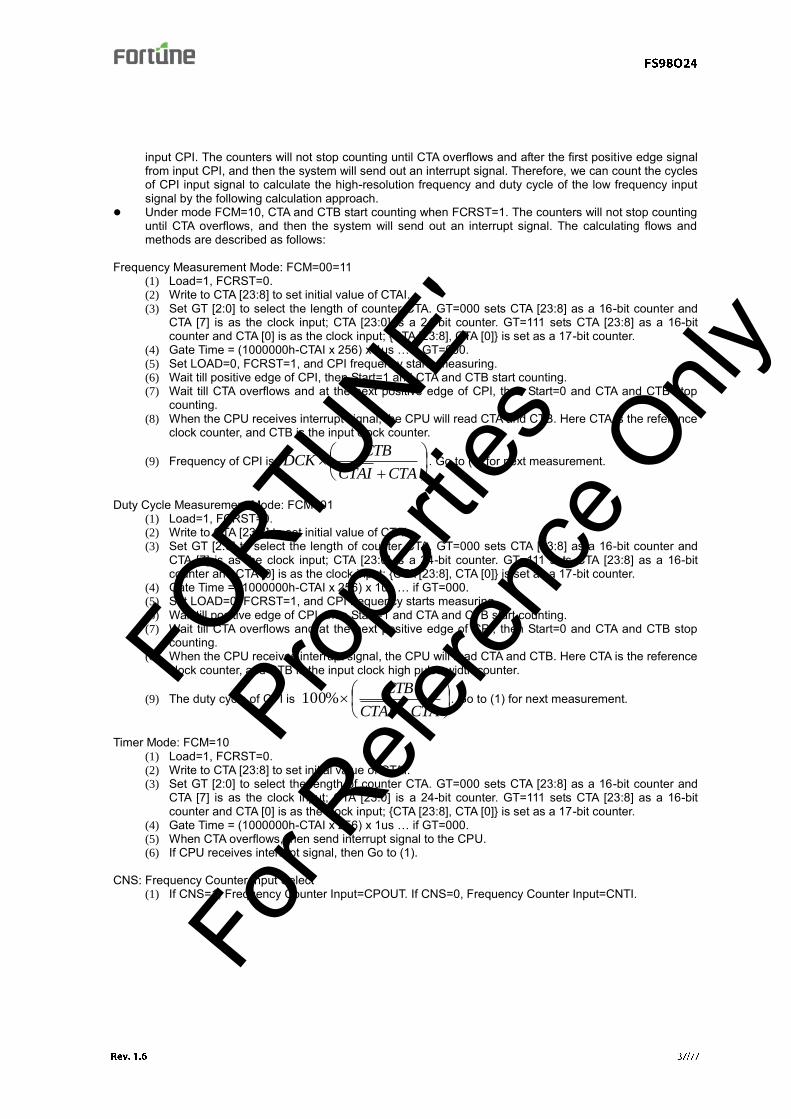
6.2. Timer Module
Table 6-2 Timer module register table
Address Name Bit 7 Bit 6 Bit 5 Bit 4 Bit 3 Bit 2 Bit 1 Bit 0 Value on Power on Reset
06H INTF TMIF -- -- -- -- 00000000 07H INTE GIE TMIE -- -- -- -- 00000000 17H TMOUT TMOUT [7:0] 00000000 18H TMCON TRST TMEN INS [2:0] 10000000
8 bits Counter
Reset
EN
CK
Out8 to 1
Mux
Timer Interrupt SignalTMOUT[7:0]
TMRST
TMEN
Frequency
Divider
TMCLK/4TMCLK
INS[2:0]
Figure 6-2 FS98O24 timer module function block
The TMCLK is same as LCD clock. LCDEN should be set to “1” if timer is in use; TMCLK frequency is set
by M5_CK and LCDCKS[1:0]. Write a “0” to bit 7 of address 18h; the CPU will send a low pulse to TRST and reset the 8-bit counter.
Then read bit 7 of 18H to get “1”. TMEN=1, the 8-bit counter will be enabled. TMEN=0, the 8-bit counter will stop. INS [2:0] selects timer interrupt source. The selection codes are as follows, 000: TMOUT [0], 001 TMOUT
Address Name Bit 7 Bit 6 Bit 5 Bit 4 Bit 3 Bit 2 Bit 1 Bit 0 Value on Power on Reset
04H STATUS -- TO -- -- -- 00u00uuu 19H WTS WDTS [2:0] 00000000
FORTU
NE'
Propert
ies
For R
eferen
ce O
nly
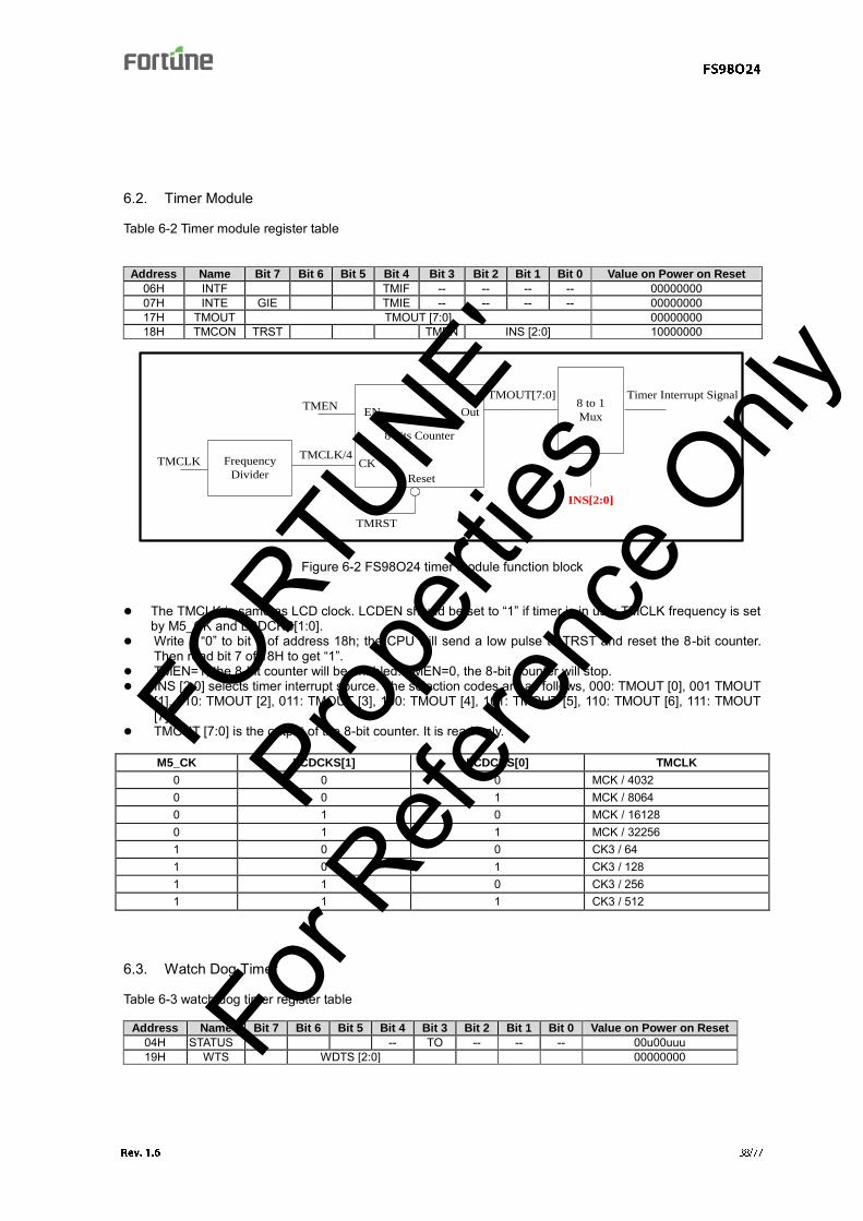
8 bits Counter1Watch Dog
Timer Oscillator
MultiplexWDTA[7:0]
WDTS[2:0]
8 bits Counter2WDTOUT
CLRWDT
Figure 6-3 watch dog timer function block
The Watchdog timer is disable during Sleep, otherwise always enable. When WDT Counter 2 overflows, it will send WDTOUT to reset the CPU and set TO flag. CLRWDT instruction will reset WDT Counter 2 WTS [2:0] selects WDT Counter 2 and the code selections are as follows, 000: WDTA [0], 001: WDTA [1],
The GPIO (General Purpose Input Output) in a micro-controller is used for general purpose input or output function. The FS98O24 GPIO includes a UART function that can be used as communication port. Users could use these ports to get digital signal or transmit data to any other digital device. Some GPIOs in FS98O24 are also defined for other special functions. In this Chapter, the GPIO will be illustrated as the GPIO function.
FORTU
NE'
Propert
ies
For R
eferen
ce O
nly
7.1. PT1
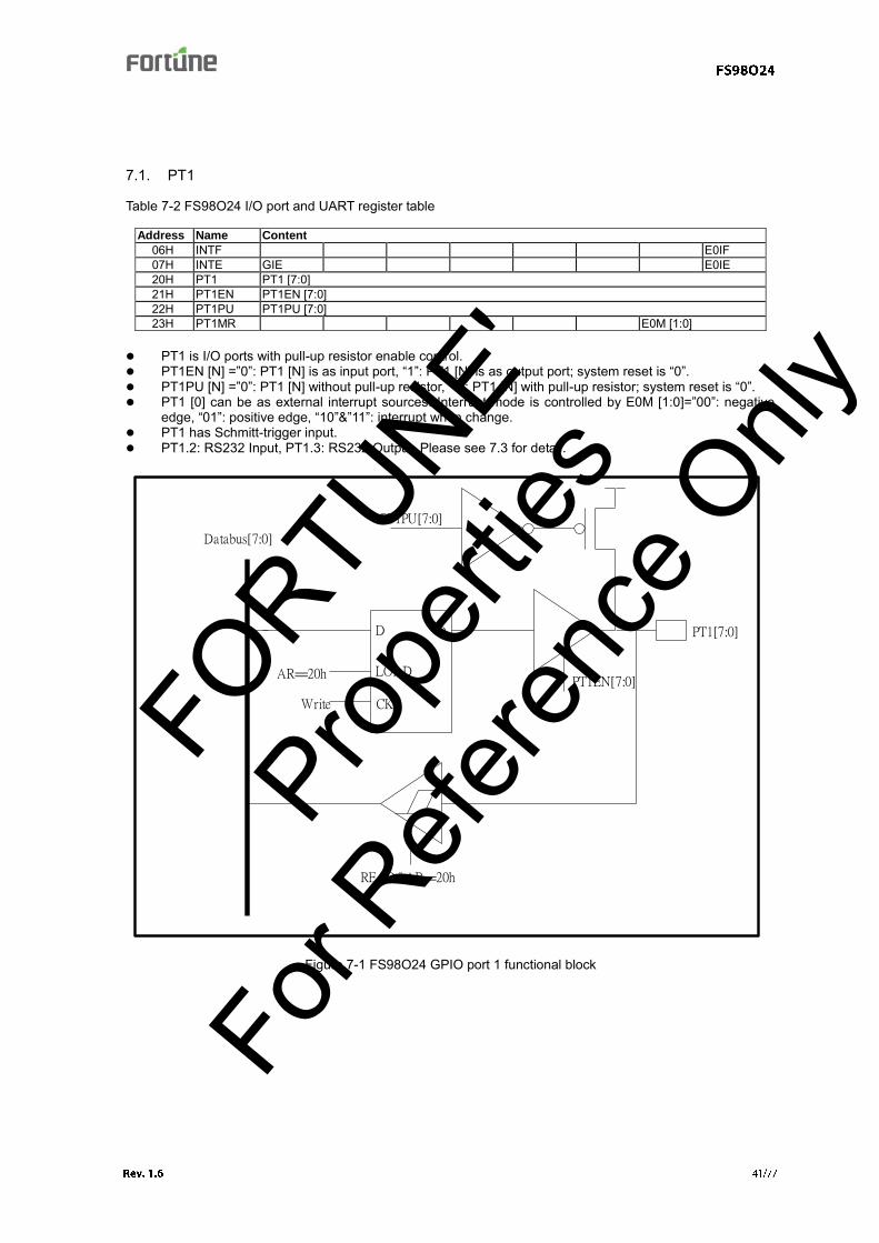
Table 7-2 FS98O24 I/O port and UART register table
PT1 is I/O ports with pull-up resistor enable control. PT1EN [N] =”0”: PT1 [N] is as input port, “1”: PT1 [N] is as output port; system reset is “0”. PT1PU [N] =”0”: PT1 [N] without pull-up resistor, “1”: PT1 [N] with pull-up resistor; system reset is “0”. PT1 [0] can be as external interrupt sources. Interrupt mode is controlled by E0M [1:0]=”00”: negative
edge, “01”: positive edge, “10”&”11”: interrupt when change. PT1 has Schmitt-trigger input. PT1.2: RS232 Input, PT1.3: RS232 Output. Please see 7.3 for detail.
PT1PU[7:0]
PT1EN[7:0]
PT1[7:0]D Q
CK
LOAD
Write
AR==20h
READ&AR==20h
Databus[7:0]
Figure 7-1 FS98O24 GPIO port 1 functional block
FORTU
NE'
Propert
ies
For R
eferen
ce O
nly
7.2. PT2
Table 7-3 FS98O24 I/O port and UART register table
Address Name Content
24H PT2 PT2 [7:0] 25H PT2EN PT2EN [7:0] 26H PT2PU PT2PU [7:0] 27H PT2MR BPSEL BCLK S_BEEP BPEN PT2 is I/O ports with pull-up resistor enable control. PT2EN [N] =”0”: PT2 [N] is as input port, “1”: PT2 [N] is as output port; system reset is “0”. PT2 has Schmitt-trigger input.
PT2PU[7:0]
PT2EN[7:0]
PT2[7:0]D Q
CK
LOAD
Write
AR==24h
READ&AR==24h
Databus[7:0]
Figure 7-2 FS98O24 GPIO port 2 functional block
FORTU
NE'
Propert
ies
For R
eferen
ce O
nly
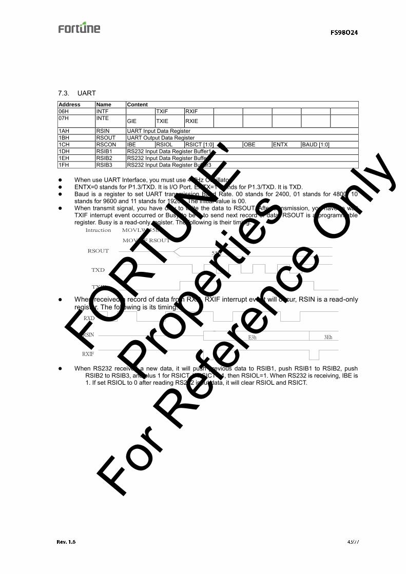
7.3. UART Address Name Content
06H INTF TXIF RXIF 07H INTE GIE TXIE RXIE
1AH RSIN UART Input Data Register 1BH RSOUT UART Output Data Register 1CH RSCON IBE RSIOL RSICT [1:0] OBE ENTX BAUD [1:0] 1DH RSIB1 RS232 Input Data Register Buffer1 1EH RSIB2 RS232 Input Data Register Buffer2 1FH RSIB3 RS232 Input Data Register Buffer3 When use UART Interface, you must use 4MHz Oscillator. ENTX=0 stands for P1.3/TXD. It is I/O Port. ENTX=1 stands for P1.3/TXD. It is TXD. Baud is a register to set UART transmission Baud Rate. 00 stands for 2400, 01 stands for 4800, 10
stands for 9600 and 11 stands for 19200. The initial value is 00. When transmit signal, you have only to write the data to RSOUT. After transmission, you have to wait
TXIF interrupt event occurred or Busy to be 0 to send next record of data. RSOUT is a programmable register. Busy is a read-only register. The following is their timing:
RSOUT
Intruction
TXD
MOVWF RSOUT
MOVLW 55h
55h
TXIF When received a record of data from RXD, RXIF interrupt event will occur, RSIN is a read-only
register. The following is its timing: RXD
RSINE3h 3Eh
RXIF
When RS232 received a new data, it will push previous data to RSIB1, push RSIB1 to RSIB2, push RSIB2 to RSIB3, and plus 1 for RSICT. If RSICT> 4, then RSIOL=1. When RS232 is receiving, IBE is 1. If set RSIOL to 0 after reading RS232 input data, it will clear RSIOL and RSICT.
FORTU
NE'
Propert
ies
For R
eferen
ce O
nly
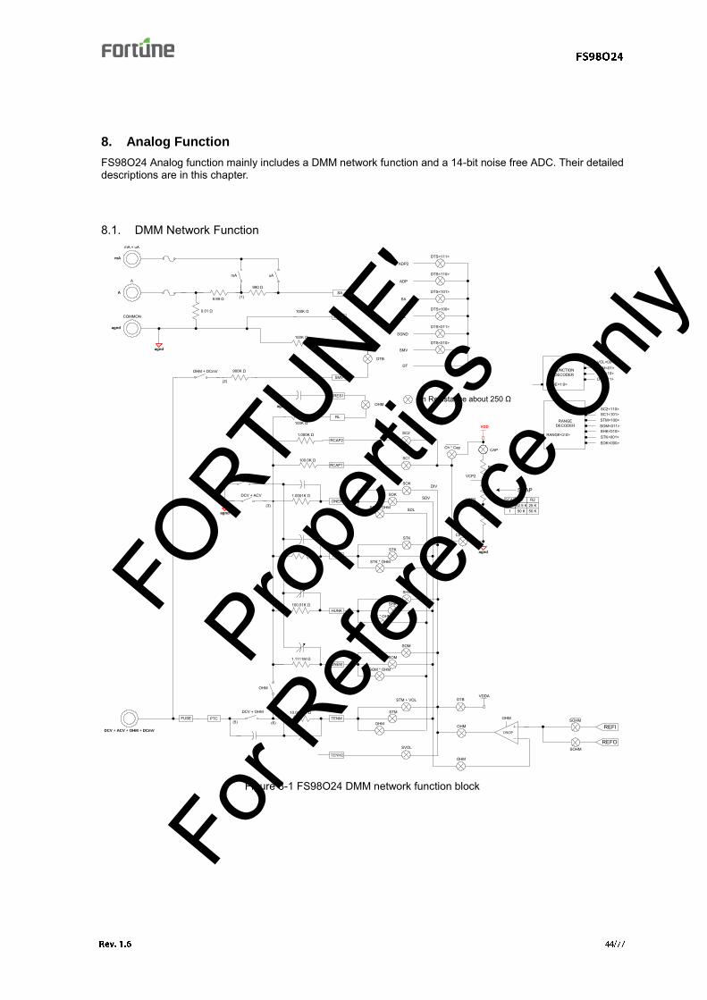
8. Analog Function
FS98O24 Analog function mainly includes a DMM network function and a 14-bit noise free ADC. Their detailed descriptions are in this chapter.
8.1. DMM Network Function
DCV + OHM
PTCFUSE
DCV + ACV + OHM + DCmV
OHM
TENK
SGND
ONEK
TENM2
ONEM
HUNK
TENM
OSOP
VDDA
SDL
DIV
REFI
SDV
SVOL
SOK
SOK
SOK * OHM
STK
STK
STK * OHM
SHK
SHK
SHK * OHM
SOM
SOM
SOM * OHM
STM + VOL
STM
OHM
DTB
OHM
OHM
OHM
DCV + ACV
ACV
RL
OHM + DCmVSMV
0.01 Ω
uA
mA + uA
COMMON
SA
mAA
DTB
DTagnd
mA
A
agnd
RCAP1
SC1
CRES1
RCAP2
SC2VDD
VCP2
VCP3
CAPCh * Cap
On Resistance about 250 Ω
RANGEDECODER
RANGE<2:0>
STM<100>SOM<011>SHK<010>STK<001>SOK<000>
SC1<101>
FUNCTIONDECODER
MODE<1:0>
VOL<00>OHM<01>CAP<10>DTB<11>
REFOSOHM
SOHM
R1
R2
R1
DTS<111>
ADP2
DT
SCAP R1 R20
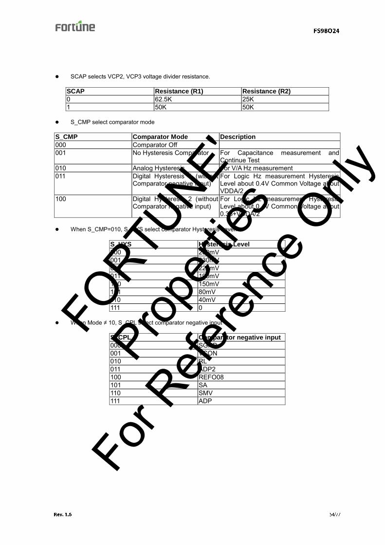
50 K 50 K162.5 K 25 K
SCAP
9.99 Ω
990 Ω
100K Ω
100K Ω
(1)
900K Ω
(2)
OHMagnd
100K Ω
1.000K Ω
100.0K Ω
Ch * Cap
DTS<110>
ADP
DTS<101>
SA
DTS<100>
RL
DTS<011>
SGND
DTS<010>
SMV
agnd
(3)
1.0001K Ω
SC2<110>
agnd10.010K Ω
100.01K Ω
1.1111M Ω
(5) (6)
10.0000M Ω
Figure 8-1 FS98O24 DMM network function block
FORTU
NE'
Propert
ies
For R
eferen
ce O
nly
Table 8-1 DMM function network register table
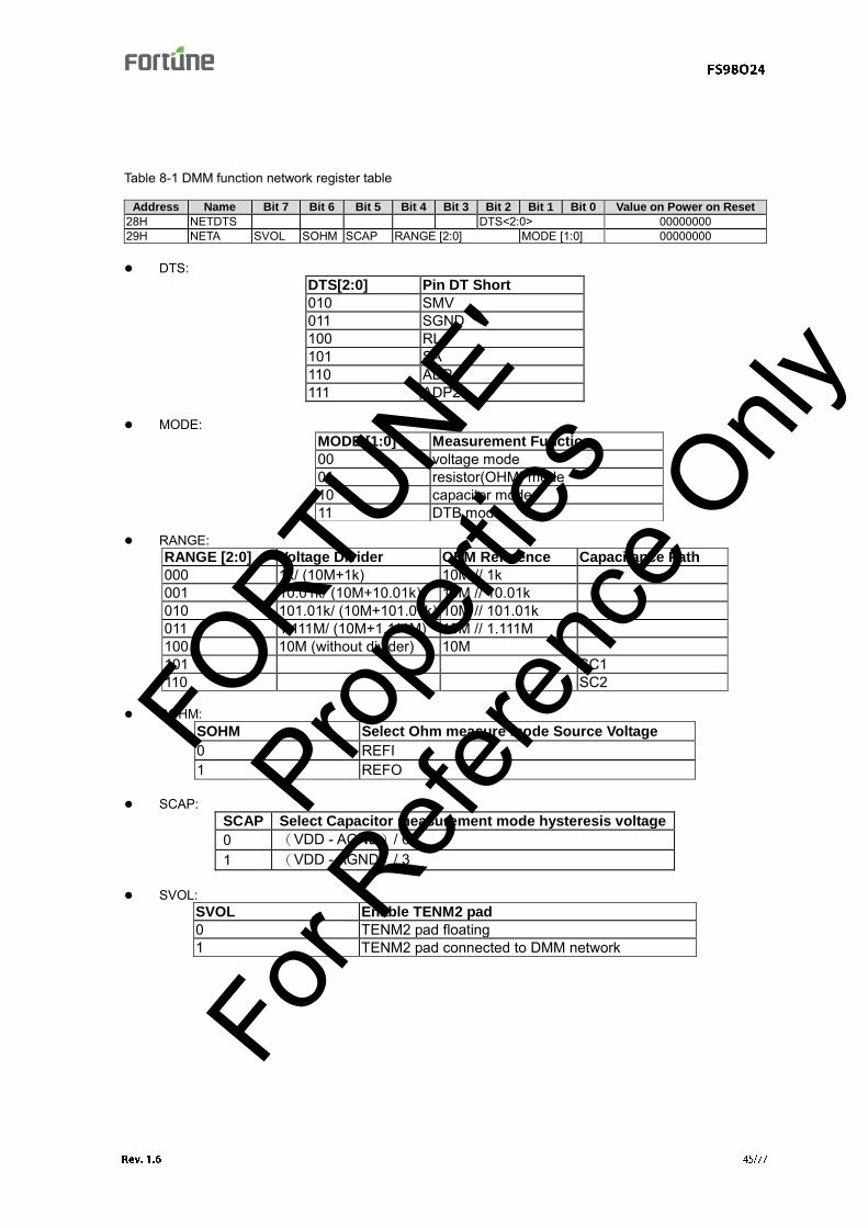
Address Name Bit 7 Bit 6 Bit 5 Bit 4 Bit 3 Bit 2 Bit 1 Bit 0 Value on Power on Reset
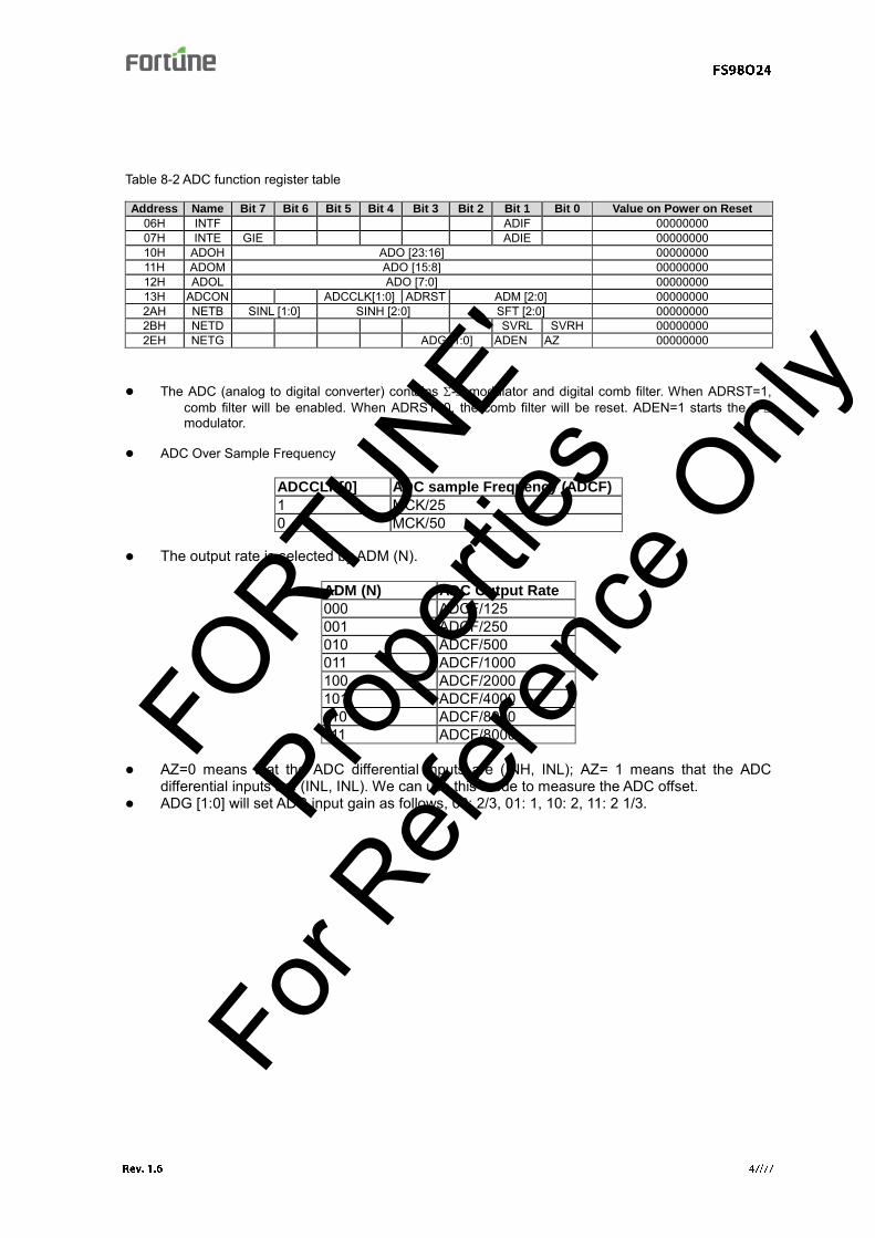
The ADC (analog to digital converter) contains - modulator and digital comb filter. When ADRST=1, comb filter will be enabled. When ADRST=0, the comb filter will be reset. ADEN=1 starts the - modulator.
AZ=0 means that the ADC differential inputs are (INH, INL); AZ= 1 means that the ADC
differential inputs are (INL, INL). We can use this mode to measure the ADC offset. ADG [1:0] will set ADC input gain as follows, 00: 2/3, 01: 1, 10: 2, 11: 2 1/3.
FORTU
NE'
Propert
ies
For R
eferen
ce O
nly
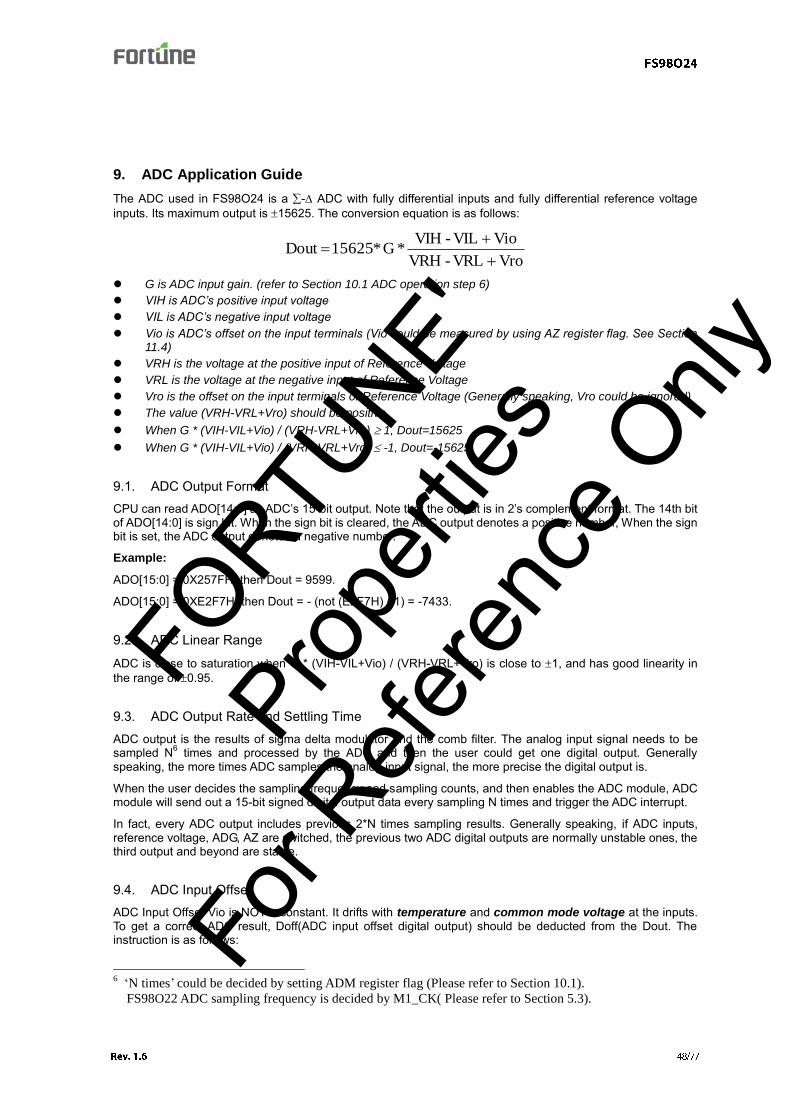
9. ADC Application Guide
The ADC used in FS98O24 is a - ADC with fully differential inputs and fully differential reference voltage inputs. Its maximum output is 15625. The conversion equation is as follows:
VroVRL-VRH
VioVIL-VIH *G * 15625 Dout
G is ADC input gain. (refer to Section 10.1 ADC operation step 6)
VIH is ADC’s positive input voltage
VIL is ADC’s negative input voltage
Vio is ADC’s offset on the input terminals (Vio could be measured by using AZ register flag. See Section 11.4)
VRH is the voltage at the positive input of Reference Voltage
VRL is the voltage at the negative input of Reference Voltage
Vro is the offset on the input terminals of Reference Voltage (Generally speaking, Vro could be ignored)
The value (VRH-VRL+Vro) should be positive.
When G * (VIH-VIL+Vio) / (VRH-VRL+Vro) 1, Dout=15625
When G * (VIH-VIL+Vio) / (VRH-VRL+Vro) -1, Dout=-15625
9.1. ADC Output Format CPU can read ADO[14:0] as ADC’s 15-bit output. Note that the output is in 2’s complement format. The 14th bit of ADO[14:0] is sign bit. When the sign bit is cleared, the ADC output denotes a positive number, When the sign bit is set, the ADC output denotes a negative number.
ADC is close to saturation when G * (VIH-VIL+Vio) / (VRH-VRL+Vro) is close to 1, and has good linearity in the range of 0.95.
9.3. ADC Output Rate and Settling Time ADC output is the results of sigma delta modulator and the comb filter. The analog input signal needs to be sampled N6 times and processed by the ADC and then the user could get one digital output. Generally speaking, the more times ADC samples the analog input signal, the more precise the digital output is.
When the user decides the sampling frequency and sampling counts, and then enables the ADC module, ADC module will send out a 15-bit signed digital output data every sampling N times and trigger the ADC interrupt.
In fact, every ADC output includes previous 2*N times sampling results. Generally speaking, if ADC inputs, reference voltage, ADG, AZ are switched, the previous two ADC digital outputs are normally unstable ones, the third output and beyond are stable.
9.4. ADC Input Offset ADC Input Offset Vio is NOT a constant. It drifts with temperature and common mode voltage at the inputs. To get a correct ADC result, Doff(ADC input offset digital output) should be deducted from the Dout. The instruction is as follows:
6 ‘N times’ could be decided by setting ADM register flag (Please refer to Section 10.1).
FS98O22 ADC sampling frequency is decided by M1_CK( Please refer to Section 5.3).
FORTU
NE'
Propert
ies
For R
eferen
ce O
nly
1. Set AZ bit, and VIH and VIL will short. Dout will be 15625 *G * (Vio) / (VRH-VRL+Vro). It’s called Doff. 2. Save Doff in memory, and then Clear AZ bit to restart the ADC module. 3. Pass the first 2 ADC interrupts for ignoring the unstable ADC result. 4. When measuring analog signal, Doff should be deducted.
9.5. ADC Digital Output The ADC digital output deducted by Doff is ADC Gain. The ADC Gain doesn’t change as VDD changes. The
suggested values for common mode voltages at ADC input and reference voltage are 1V~2V.
ADC input gain could be set by ADG[1:0] register flag. Please see Section 10.1 for detail.
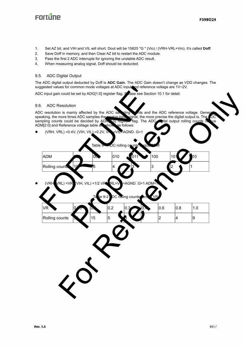
9.6. ADC Resolution ADC resolution is mainly affected by the ADC sampling counts and the ADC reference voltage. Generally speaking, the more times ADC samples the analog input signal, the more precise the digital output is. The ADC sampling counts could be decided by ADM[2:0] register flag. The ADC digital output rolling counts versus ADM[2:0] and Reference voltage table are shown as follows:
The input noise of CMOS OPAMP is generally much larger than the one of a Bipolar OPAMP. Moreover, the flick noise (1/f noise) of CMOS is a killer for low frequency small signal measurement. But the need for input bias current in Bipolar OPAMP causes that some transducers can not be used. In general, bipolar process is not good for highly integrated ICs. FS98O24 use special CMOS low noise circuit design, and under normal conditions, the input noise is controlled under 1μVpp (0.1Hz~1Hz). FS98O24 is good for transducer applications because there is no need to consider input bias current.
Most of the input noise in CMOS OPAMP comes from input differential amplification. S_CHCK can be set to switch the differential amplification: 00 for positive Offset Voltage, 01 for negative Offset voltage. When using one clock pulse to switch input differential amplification, that is called chopper mode. In general, chopper frequency is set between 1 KHz and 2 KHz.
Under chopper mode, the input noise peak-to-peak voltage in FS98O24 is less than 0.5μV (0.1Hz~1Hz). But an equivalent input current of less than 100pA is generated, due to the effect of switching.
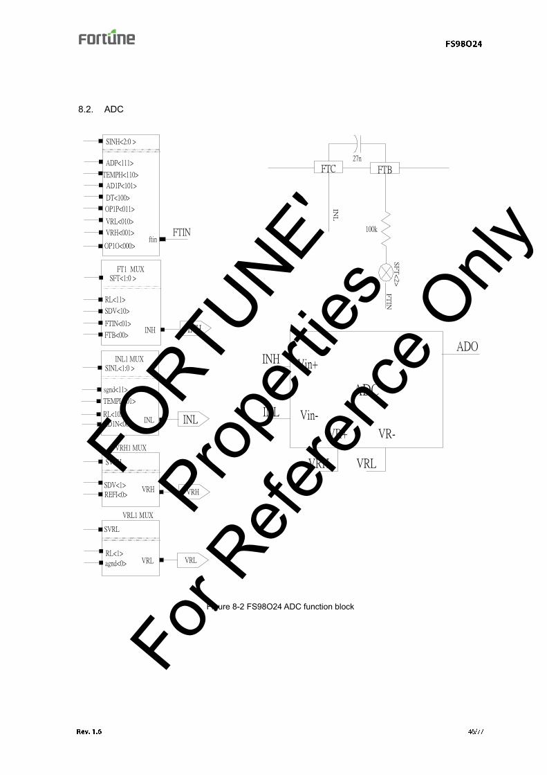
Figure 10-1 The FS98O24 OPAMP functional block
+
-
OP
1O
OP
1N
+
-
OP
2O
OP
2N
OP
2P
SOP1P<2:0 >
SGND<111>
AGND<110>
ADP2<101>
ADP<100> OP1P
SA<010>
RL<001>
SDV<011>
SMV<000>
OP1EN S_CH1CK[1:0]S_CH2CK[1:0]OP2EN
SONE
SO
NE
FORTU
NE'
Propert
ies
For R
eferen
ce O
nly
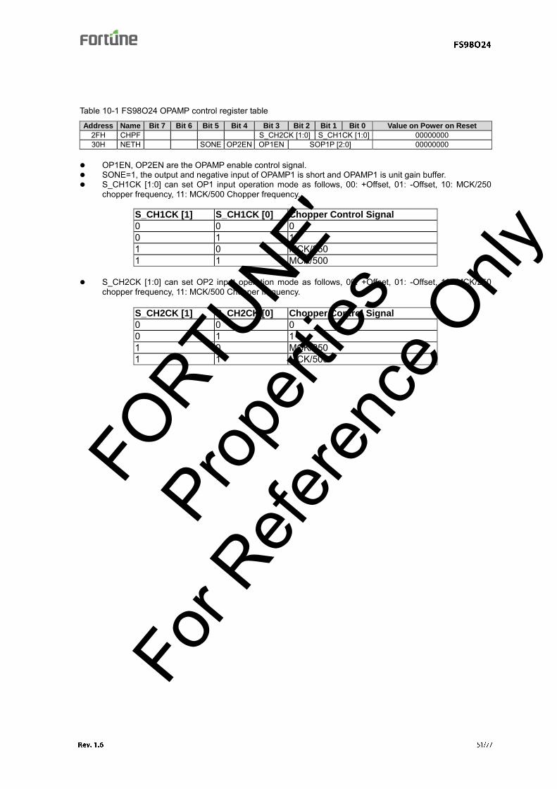
Table 10-1 FS98O24 OPAMP control register table
Address Name Bit 7 Bit 6 Bit 5 Bit 4 Bit 3 Bit 2 Bit 1 Bit 0 Value on Power on Reset
OP1EN, OP2EN are the OPAMP enable control signal. SONE=1, the output and negative input of OPAMP1 is short and OPAMP1 is unit gain buffer. S_CH1CK [1:0] can set OP1 input operation mode as follows, 00: +Offset, 01: -Offset, 10: MCK/250
chopper frequency, 11: MCK/500 Chopper frequency.
S_CH1CK [1] S_CH1CK [0] Chopper Control Signal
0 0 0 0 1 1 1 0 MCK/250 1 1 MCK/500
S_CH2CK [1:0] can set OP2 input operation mode as follows, 00: +Offset, 01: -Offset, 10: MCK/250
chopper frequency, 11: MCK/500 Chopper frequency.
S_CH2CK [1] S_CH2CK [0] Chopper Control Signal
0 0 0 0 1 1 1 0 MCK/250 1 1 MCK/500
FORTU
NE'
Propert
ies
For R
eferen
ce O
nly
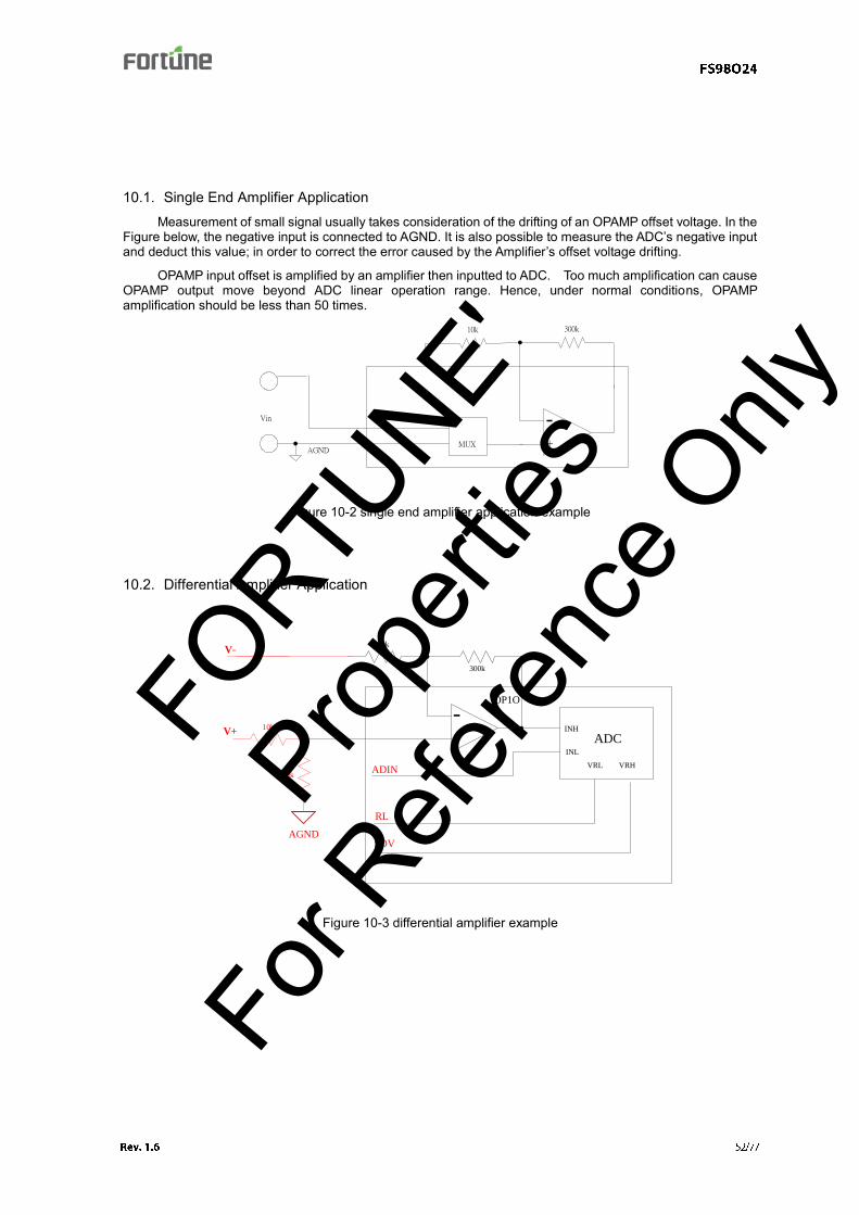
10.1. Single End Amplifier Application Measurement of small signal usually takes consideration of the drifting of an OPAMP offset voltage. In the
Figure below, the negative input is connected to AGND. It is also possible to measure the ADC’s negative input and deduct this value; in order to correct the error caused by the Amplifier’s offset voltage drifting.
OPAMP input offset is amplified by an amplifier then inputted to ADC. Too much amplification can cause OPAMP output move beyond ADC linear operation range. Hence, under normal conditions, OPAMP amplification should be less than 50 times.
300k10k
AGND
Vin
+
-MUX
Figure 10-2 single end amplifier application example
10.2. Differential Amplifier Application
V-
300k
10k
+
-OP1O
300k
10k
ADCINH
INL
VRHVRL
RL
SDV
ADIN
V+
AGND
Figure 10-3 differential amplifier example
FORTU
NE'
Propert
ies
For R
eferen
ce O
nly
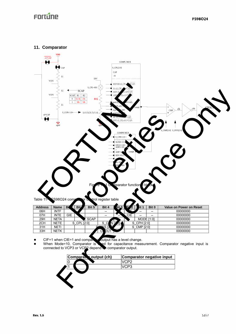
11. Comparator
+
-
80 K
1k/10.5k/26.7k/31.6k
agnd
S_CPL=001
ch*CAP
agnd
VDD
VCP2
VCP3
CAP
ch*CAP
S_CON<1:0>
SCAP
sgnd (S_CPL=000*CAP)
compl(S_CPL=001*CAP)
vcp2 (ch*CAP)
vcp3 (ch*CAP)
RL (S_CPL=010*CAP)
ADP2 (S_CPL=011*CAP)
COMPH MUX
S_CPH<2:0 >
SGND<111>
OP1O<110>ADP2<101
>ADP<100> comph
SA<010>
RL<001>
SDV<011>
SMV<000>
R2
R1
R1
CPOUTch chb
CMP
S_CMP[2:0] S_HYS[2:0]
DIV
COMPL MUX
S_CPL[2:0]
CAP
ch
REFO08 (S_CPL=100*CAP)
SA (S_CPL=101*CAP)
SMV (S_CPL=110*CAP)
ADP (S_CPL=111*CAP)SCAP R1 R2
0
50k 50k1
62.5k 25k
Figure 11-1 Comparator functional block
Table 11-1 FS98O24 comparator control register table
Address Name Bit 7 Bit 6 Bit 5 Bit 4 Bit 3 Bit 2 Bit 1 Bit 0 Value on Power on Reset
When S_CPL=001, VCON is continuity test comparison voltage. The voltage level is decided by voltage divider. The voltage divider ratio is selected by S_CON.
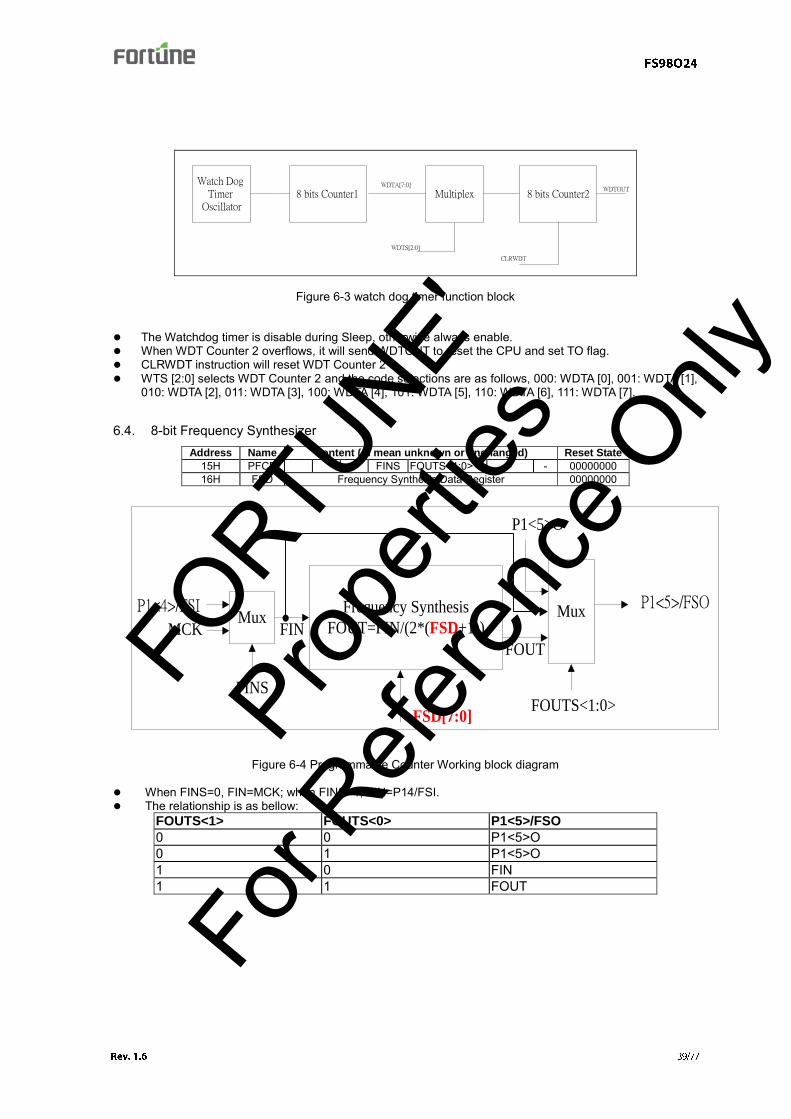
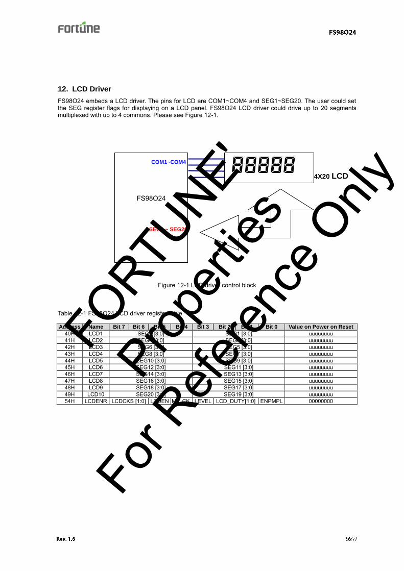
FS98O24 embeds a LCD driver. The pins for LCD are COM1~COM4 and SEG1~SEG20. The user could set the SEG register flags for displaying on a LCD panel. FS98O24 LCD driver could drive up to 20 segments multiplexed with up to 4 commons. Please see Figure 12-1.
Figure 12-1 LCD driver control block
Table 12-1 FS98O24 LCD driver register table
Address Name Bit 7 Bit 6 Bit 5 Bit 4 Bit 3 Bit 2 Bit 1 Bit 0 Value on Power on Reset
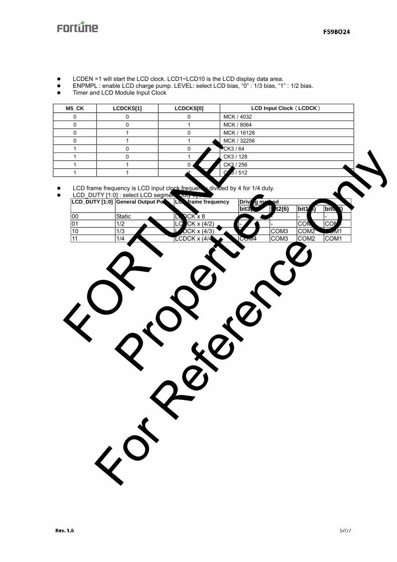
LCD frame frequency is LCD input clock frequency divided by 4 for 1/4 duty. LCD_DUTY [1:0] : select LCD segment Duty cycle.
LCD_DUTY [1:0] General Output Port LCD frame frequency Driving method
bit3(7) bit2(6) bit1(5) bit0(4)
00 Static LCDCK x 8 - - - - 01 1/2 LCDCK x (4/2) - - COM2 COM1 10 1/3 LCDCK x (4/3) - COM3 COM2 COM1 11 1/4 LCDCK x (4/4) COM4 COM3 COM2 COM1
FORTU
NE'
Propert
ies
For R
eferen
ce O
nly
LCD Driving Methods : There are six kinds of LCD driving methods and they can be selected by LCD_DUTY[1:0] and LEVEL . The output waveforms of LCD driver are as below : (VDD=3.0V)
COM1
COM2
COM3
V3
V2
V1
VSS
LCD segments ONCOM1 side lighted
(1) 1/4 duty, 1/3 bias
VDD
V3
V2
V1
VSSLCB
LCA
3V
2V
1V
VDD
V3
V2
V1
VSSLCB
LCA
4.5V
3V
1.5V
Frame
LCD segments OFF
(2) 1/3 duty, 1/3 bias
V3
V2
V1
VSS
V3
V2
V1
VSS
V3
V2
V1
VSS
V3
V2
V1
VSS
V3
V2
V1
VSS
VDD
V3
V2
V1
VSSLCB
LCA
3V
2V
1V
VDD
V3
V2
V1
VSSLCB
LCA
4.5V
3V
1.5V
Frame
V3
V2
V1
VSS
V3
V2
V1
VSS
V3
V2
V1
VSS
V3
V2
V1
VSS
V3
V2
V1
VSS
COM4
V3
V2
V1
VSS
FORTU
NE'
Propert
ies
For R
eferen
ce O
nly
COM1
COM2
COM3
COM4
V2
V1
VSS
LCD segments ONCOM1 side lighted
(3) 1/4 duty, 1/2 bias
VDD
V3
V2
V1
VSSLCB
LCA
3V
1.5V
Frame
LCD segments OFF
(4) 1/3 duty, 1/2 bias
V2
V1
VSS
V2
V1
VSS
V2
V1
VSS
V1
VSS
V2
V1
VSS
VDD
V3
V2
V1
VSSLCB
LCA
3V
1.5V
V2
V2
V1
VSS
Frame
V2
V1
VSS
V2
V1
VSS
V1
VSS
V2
V1
VSS
V2
V2
V1
VSS
FORTU
NE'
Propert
ies
For R
eferen
ce O
nly
COM1
COM2
COM3
COM4
V2
V1
VSS
LCD segments ONCOM1 side lighted
(5) 1/2 duty, 1/2 bias
VDD
V3
V2
V1
VSSLCB
LCA
3V
1.5V
Frame
LCD segments OFF
(6) static
V2
V1
VSS
V1
VSS
V2
V1
VSS
VDD
V3
V2
V1
VSSLCB
LCA
3V
1V
V2
V2
V1
VSS
V2
V1
VSS
VDD
V3
V2
V1
VSSLCB
LCA
3V
1.5V
V2
V1
VSS
V2
V1
VSS
V2
V1
VSS
V1
VSS
V2
V1
VSS
V2
V1
VSS
V2
2V
V3
V2
V1
VSS
V3
V2
V1
VSS
V3
V2
V1
VSS
V3
V2
V1
VSS
V3
V2
V1
VSS
V3
V2
V1
VSS
FORTU
NE'
Propert
ies
For R
eferen
ce O
nly
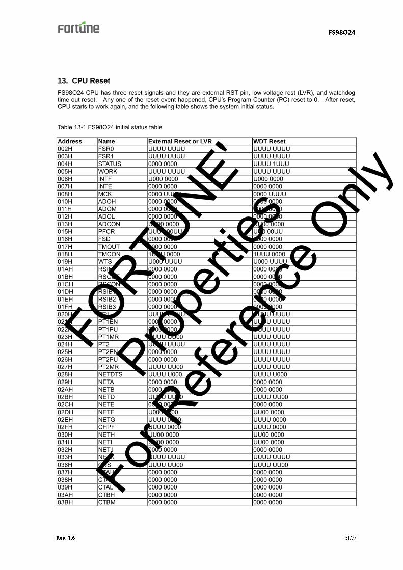
13. CPU Reset
FS98O24 CPU has three reset signals and they are external RST pin, low voltage rest (LVR), and watchdog time out reset. Any one of the reset event happened, CPU’s Program Counter (PC) reset to 0. After reset, CPU starts to work again, and the following table shows the system initial status.
FS98O24 supports low power working mode. When the user want FS98O24 to do nothing and just stand by, FS98O24 could be set to Halt mode or Sleep mode to reduce the power consumption by stopping the CPU core working. The two modes will be described below.
Halt Mode
After CPU executes a Halt command, CPU Program Counter (PC) stops counting until an interrupt command is issued. To avoid program errors caused by Interrupt Return, it is suggested to add a NOP command after Halt to guarantee the program’s normal execution when turning back.
Sleep Mode
After CPU executes Sleep command, all oscillators stop working until an external interrupt command is issued or the CPU is reset. To avoid program errors caused by Interrupt return, it is suggested to add a NOP command after Sleep to guarantee the program’s normal execution. The sleep mode power consumption is about 3 uA.
To make sure that CPU consumes minimum power in Sleep mode, it is necessary to close all power blocks and analog circuits before issuing the Sleep command, and make sure that all I/O Ports are in VDD or VSS voltage levels.
It is recommended that users execute the following program before issuing the Sleep command:
CLRF NETA ; As Reset state CLRF NETB ; As Reset state CLRF NETC ; As Reset state CLRF NETD ; As Reset state CLRF NETE ; As Reset state CLRF NETF ; As Reset state CLRF PT2PU ; Pull up resistor is disconnected. MOVLW 0FFH MOVWF PT2EN ; PT2 ports are assigned to be output ports. CLRF PT2 ; Set PT2 ports Output Low. MOVLW 001h MOVWF PT1PU ; PT1 Pull up resistor is disconnected except port 0(ext. int) MOVLW 0FEh MOVWF PT1EN ; PT1 ports are assigned to be output ports except port 0 CLRF PT1 ; Set PT1 [7:1] Output Low CLRF INTF ; Clear the interrupt flags MOVLW 081h MOVWF INTE ; Enable the external interrupt SLEEP ; Set the FWZ0038A into Sleep mode NOP ; Wait CPU Wake-Up to normal Run
FORTU
NE'
Propert
ies
For R
eferen
ce O
nly
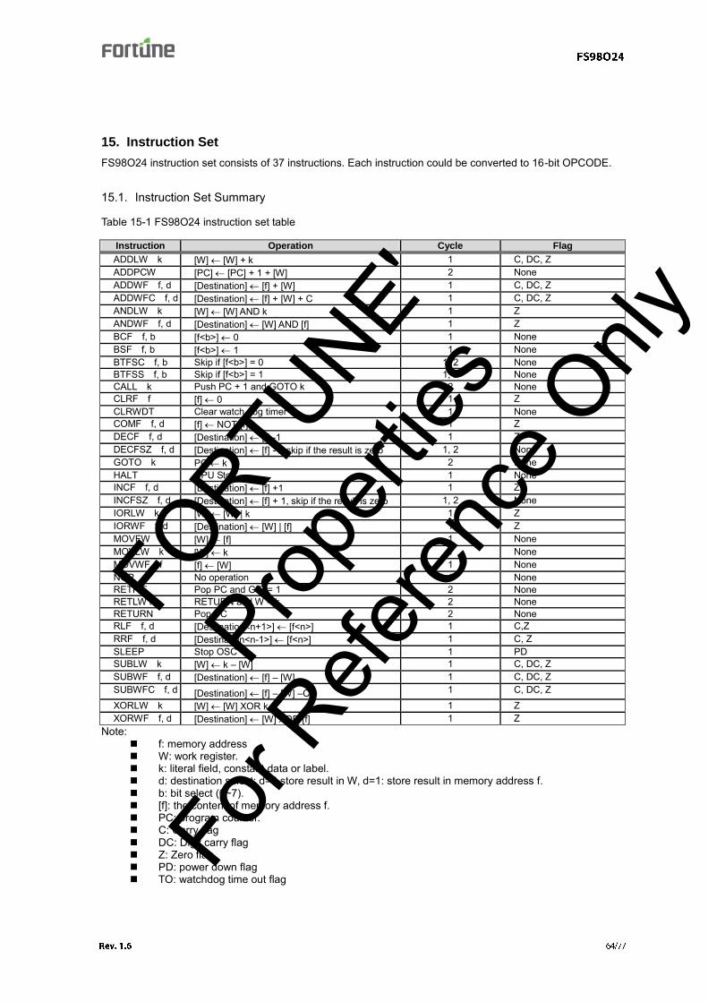
15. Instruction Set
FS98O24 instruction set consists of 37 instructions. Each instruction could be converted to 16-bit OPCODE.
15.1. Instruction Set Summary
Table 15-1 FS98O24 instruction set table Instruction Operation Cycle Flag
ADDLW k [W] [W] + k 1 C, DC, Z ADDPCW [PC] [PC] + 1 + [W] 2 None ADDWF f, d [Destination] [f] + [W] 1 C, DC, Z ADDWFC f, d [Destination] [f] + [W] + C 1 C, DC, Z ANDLW k [W] [W] AND k 1 Z ANDWF f, d [Destination] [W] AND [f] 1 Z BCF f, b [f<b>] 0 1 None BSF f, b [f<b>] 1 1 None BTFSC f, b Skip if [f<b>] = 0 1, 2 None BTFSS f, b Skip if [f<b>] = 1 1, 2 None CALL k Push PC + 1 and GOTO k 2 None CLRF f [f] 0 1 Z CLRWDT Clear watch dog timer 1 None COMF f, d [f] NOT([f]) 1 Z DECF f, d [Destination] [f] -1 1 Z DECFSZ f, d [Destination] [f] -1, skip if the result is zero 1, 2 None GOTO k PC k 2 None HALT CPU Stop 1 None INCF f, d [Destination] [f] +1 1 Z INCFSZ f, d [Destination] [f] + 1, skip if the result is zero 1, 2 None IORLW k [W] [W] | k 1 Z IORWF f, d [Destination] [W] | [f] 1 Z MOVFW f [W] [f] 1 None MOVLW k [W] k 1 None MOVWF f [f] [W] 1 None NOP No operation 1 None RETFIE Pop PC and GIE = 1 2 None RETLW k RETURN and W = k 2 None RETURN Pop PC 2 None RLF f, d [Destination<n+1>] [f<n>] 1 C,Z RRF f, d [Destination<n-1>] [f<n>] 1 C, Z SLEEP Stop OSC 1 PD SUBLW k [W] k – [W] 1 C, DC, Z SUBWF f, d [Destination] [f] – [W] 1 C, DC, Z SUBWFC f, d [Destination] [f] – [W] –C‧ 1 C, DC, Z XORLW k [W] [W] XOR k 1 Z XORWF f, d [Destination] [W] XOR [f] 1 Z
Note: f: memory address W: work register. k: literal field, constant data or label. d: destination select: d=0 store result in W, d=1: store result in memory address f. b: bit select (0~7). [f]: the content of memory address f. PC: program counter. C: Carry flag DC: Digit carry flag Z: Zero flag PD: power down flag TO: watchdog time out flag
FORTU
NE'
Propert
ies
For R
eferen
ce O
nly
15.2. Instruction Description
(By alphabetically) ADDLW Add Literal to W Syntax ADDLW k
0 k FFh Operation [W] [W] + k Flag Affected C, DC, Z Description The content of Work register add literal “k” in Work register Cycle 1 Example: ADDLW 08h
Before instruction: W = 08h
After instruction: W = 10h
ADDPCW Add W to PC Syntax ADDPCW Operation [PC] [PC] + 1 + [W], [W] < 7Fh
[PC] [PC] + 1 + ([W] – 100h), otherwise Flag Affected None Description The relative address PC + 1 + W are loaded into PC. Cycle 2 Example 1: ADDPCW
Before instruction: W = 7Fh, PC = 0212h
After instruction: PC = 0292h
Example 2: ADDPCW
Before instruction: W = 80h, PC = 0212h
After instruction: PC = 0193h
Example 3: ADDPCW
Before instruction: W = FEh, PC = 0212h
After instruction: PC = 0211h
ADDWF Add W to f Syntax ADDWF f, d
0 f FFh d [0,1]
Operation [Destination] [f] + [W] Flag Affected C, CD, Z Description Add the content of the W register and [f]. If d is 0, the result is stored in the W register.
If d is 1, the result is stored back in f. Cycle 1 Example 1: ADDWF OPERAND, 0
Before instruction: OPERAND = C2h W = 17h
After instruction: OPERAND = C2h W = D9h
Example 2: ADDWF OPERAND, 1
Before instruction: OPERAND = C2h W = 17h
After instruction: OPERAND = D9h W = 17h
FORTU
NE'
Propert
ies
For R
eferen
ce O
nly
ADDWFC Add W, f and Carry Syntax ADDWFC f, d
0 f FFh d [0,1]
Operation [Destination] [f] + [W] + C Flag Affected C, DC, Z Description Add the content of the W register, [f] and Carry bit.
If d is 0, the result is stored in the W register. If d is 1, the result is stored back in f.
Cycle 1 Example ADDWFC OPERAND,1
Before instruction: C = 1 OPERAND = 02h W = 4Dh
After instruction:
C = 0 OPERAND = 50h W = 4Dh
ANDLW AND literal with W Syntax ANDLW k
0 k FFh Operation [W] [W] AND k Flag Affected Z Description AND the content of the W register with the eight-bit literal "k".
The result is stored in the W register. Cycle 1 Example: ANDLW 5Fh
Before instruction: W = A3h
After instruction: W = 03h
ANDWF AND W and f Syntax ANDWF f, d
0 f FFh d [0,1]
Operation [Destination] [W] AND [f] Flag Affected Z Description AND the content of the W register with [f].
If d is 0, the result is stored in the W register. If d is 1, the result is stored back in f.
Cycle 1 Example 1: ANDWF OPERAND,0
Before instruction: W = 0Fh, OPERAND = 88h
After instruction: W = 08h, OPERAND = 88h
Example 2: ANDWF OPERAND,1
Before instruction: W = 0Fh, OPERAND = 88h
After instruction: W = 88h, OPERAND = 08h
FORTU
NE'
Propert
ies
For R
eferen
ce O
nly
BCF Bit Clear f Syntax BCF f, b
0 f FFh 0 b 7
Operation [f<b>] 0 Flag Affected None Description Bit b in [f] is reset to 0. Cycle 1 Example: BCF FLAG, 2
Before instruction: FLAG = 8Dh
After instruction: FLAG = 89h
BSF Bit Set f Syntax BSF f, b
0 f FFh 0 b 7
Operation [f<b>] 1 Flag Affected None Description Bit b in [f] is set to 1. Cycle 1 Example: BSF FLAG, 2
Before instruction: FLAG = 89h
After instruction: FLAG = 8Dh
BTFSC Bit Test skip if Clear Syntax BTFSC f, b
0 f FFh 0 b 7
Operation Skip if [f<b>] = 0 Flag Affected None Description If bit 'b' in [f] is 0, the next fetched instruction is discarded and a NOP is executed
instead making it a two-cycle instruction. Cycle 1, 2 Example: Node BTFSC FLAG, 2
OP1 : OP2 :
Before instruction: PC = address (Node)
After instruction: If FLAG<2> = 0 PC = address(OP2) If FLAG<2> = 1 PC = address(OP1)
BTFSS Bit Test skip if Set Syntax BTFSS f, b
0 f FFh 0 b 7
Operation Skip if [f<b>] = 1 Flag Affected None Description If bit 'b' in [f] is 1, the next fetched instruction is discarded and a NOP is executed
instead making it a two-cycle instruction. Cycle 1, 2 Example: Node BTFSS FLAG, 2
OP1 : OP2 :
Before instruction: PC = address (Node)
After instruction: If FLAG<2> = 0 PC = address(OP1) If FLAG<2> = 1 PC = address(OP2)
FORTU
NE'
Propert
ies
For R
eferen
ce O
nly
CALL Subroutine CALL Syntax CALL k
0 k 1FFFh Operation Push Stack
[Top Stack] PC + 1 PC k
Flag Affected None Description Subroutine Call. First, return address PC + 1 is pushed onto the stack. The immediate
address is loaded into PC. Cycle 2 CLRF Clear f Syntax CLRF f
0 f 255 Operation [f] 0 Flag Affected None Description Reset the content of memory address f Cycle 1 Example: CLRF WORK
Before instruction: WORK = 5Ah
After instruction: WORK = 00h
CLRWDT Clear watch dog timer Syntax CLRWDT Operation Watch dog timer counter will be reset Flag Affected None Description CLRWDT instruction will reset watch dog timer counter. Cycle 1 Example: CLRWDT
After instruction: WDT = 0
COMF Complement f Syntax COMF f, d
0 f 255 d [0,1]
Operation [f] NOT([f]) Flag Affected Z Description [f] is complemented. If d is 0, the result is stored in the W register. If d is 1, the result is
stored back in [f] Cycle 1 Example 1: COMF OPERAND,0
Before instruction: W = 88h, OPERAND = 23h
After instruction: W = DCh, OPERAND = 23h
Example 2: COMF OPERAND,1
Before instruction: W = 88h, OPERAND = 23h
After instruction: W = 88h, OPERAND = DCh
FORTU
NE'
Propert
ies
For R
eferen
ce O
nly
DECF Decrement f Syntax DECF f, d
0 f 255 d [0,1]
Operation [Destination] [f] -1 Flag Affected Z Description [f] is decremented. If d is 0, the result is stored in the W register. If d is 1, the result is
stored back in [f]. Cycle 1 Example 1: DECF OPERAND,0
Before instruction: W = 88h, OPERAND = 23h
After instruction: W = 22h, OPERAND = 23h
Example 2: DECF OPERAND,1
Before instruction: W = 88h, OPERAND = 23h
After instruction: W = 88h, OPERAND = 22h
DECFSZ Decrement f, skip if zero Syntax DECFSZ f, d
0 f FFh d [0,1]
Operation [Destination] [f] -1, skip if the result is zero Flag Affected None Description [f] is decremented. If d is 0, the result is stored in the W register. If d is 1, the result is
stored back in [f]. If the result is 0, then the next fetched instruction is discarded and a NOP is executed instead making it a two-cycle instruction.
After instruction: [FLAG] = [FLAG] - 1 If [FLAG] = 0 PC = address(OP2) If [FLAG] 0 PC = address(OP1)
GOTO Unconditional Branch Syntax GOTO k
0 k 1FFFh Operation PC k Flag Affected None Description The immediate address is loaded into PC. Cycle 2 HALT Stop CPU Core Clock Syntax HALT Operation CPU Stop Flag Affected None Description CPU clock is stopped. Oscillator is running. CPU can be waked up by internal and
external interrupt sources. Cycle 1
FORTU
NE'
Propert
ies
For R
eferen
ce O
nly
INCF Increment f Syntax INCF f, d
0 f FFh d [0,1]
Operation [Destination] [f] +1 Flag Affected Z Description [f] is incremented. If d is 0, the result is stored in the W register. If d is 1, the result is
stored back in [f]. Cycle 1 Example 1: INCF OPERAND,0
Before instruction: W = 88h, OPERAND = 23h
After instruction: W = 24h, OPERAND = 23h
Example 2: INCF OPERAND,1
Before instruction: W = 88h, OPERAND = 23h
After instruction: W = 88h, OPERAND = 24h
INCFSZ Increment f, skip if zero Syntax INCFSZ f, d
0 f FFh d [0,1]
Operation [Destination] [f] + 1, skip if the result is zero Flag Affected None Description [f] is incremented. If d is 0, the result is stored in the W register. If d is 1, the result is
stored back in [f]. If the result is 0, then the next fetched instruction is discarded and a NOP is executed instead making it a two-cycle instruction.
Cycle 1, 2 Example: Node INCFSZ FLAG, 1
OP1 : OP2 :
Before instruction: PC = address (Node)
After instruction: [FLAG] = [FLAG] + 1 If [FLAG] = 0 PC = address(OP2) If [FLAG] 0 PC = address(OP1)
IORLW Inclusive OR literal with W Syntax IORLW k
0 k FFh Operation [W] [W] | k Flag Affected Z Description Inclusive OR the content of the W register and the eight-bit literal "k". The result is
stored in the W register. Cycle 1 Example: IORLW 85h
Before instruction: W = 69h
After instruction: W = EDh
FORTU
NE'
Propert
ies
For R
eferen
ce O
nly
IORWF Inclusive OR W with f Syntax IORWF f, d
0 f FFh d [0,1]
Operation [Destination] [W] | [f] Flag Affected Z Description Inclusive OR the content of the W register and [f]. If d is 0, the result is stored in the W
register. If d is 1, the result is stored back in [f]. Cycle 1 Example: IORWF OPERAND,1
Before instruction: W = 88h, OPERAND = 23h
After instruction: W = 88h, OPERAND = ABh
MOVFW Move f to W Syntax MOVFW f
0 f FFh Operation [W] [f] Flag Affected None Description Move data from [f] to the W register. Cycle 1 Example: MOVFW OPERAND
Before instruction: W = 88h, OPERAND = 23h
After instruction: W = 23h, OPERAND = 23h
MOVLW Move literal to W Syntax MOVLW k
0 k FFh Operation [W] k Flag Affected None Description Move the eight-bit literal "k" to the content of the W register. Cycle 1 Example: MOVLW 23h
Before instruction: W = 88h
After instruction: W = 23h
MOVWF Move W to f Syntax MOVWF f
0 f FFh Operation [f] [W] Flag Affected None Description Move data from the W register to [f]. Cycle 1 Example: MOVWF OPERAND
Before instruction: W = 88h, OPERAND = 23h
After instruction: W = 88h, OPERAND = 88h
NOP No Operation Syntax NOP Operation No Operation Flag Affected None Description No operation. NOP is used for one instruction cycle delay. Cycle 1
FORTU
NE'
Propert
ies
For R
eferen
ce O
nly
RETFIE Return from Interrupt Syntax RETFIE Operation [Top Stack] => PC
Pop Stack 1 => GIE
Flag Affected None Description The program counter is loaded from the top stack, then pop stack. Setting the GIE bit
enables interrupts. Cycle 2 RETLW Return and move literal to W Syntax RETLW k
0 k FFh Operation [W] k
[Top Stack] => PC Pop Stack
Flag Affected None Description Move the eight-bit literal "k" to the content of the W register. The program counter is
loaded from the top stack, then pop stack. Cycle 2 Return Return from Subroutine Syntax RETURN Operation [Top Stack] => PC
Pop Stack Flag Affected None Description The program counter is loaded from the top stack, then pop stack. Cycle 2 RLF Rotate left [f] through Carry Syntax RLF f, d
0 f FFh d [0,1]
Operation
[Destination<n+1>] [f<n>] [Destination<0>] C C [f<7>]
Flag Affected C, Z Description
C Register f
[f] is rotated one bit to the left through the Carry bit. If d is 0, the result is stored in the W register. If d is 1, the result is stored back in [f].
Cycle 1 Example: RLF OPERAND, 1
Before instruction: C = 0 W = 88h, OPERAND = E6h
After instruction: C = 1 W = 88h, OPERAND = CCh
FORTU
NE'
Propert
ies
For R
eferen
ce O
nly
RRF Rotate right [f] through Carry Syntax RRF f, d
0 f FFh d [0,1]
Operation [Destination<n-1>] [f<n>] [Destination<7>] C C [f<7>]
Flag Affected C Description
C Register f
[f] is rotated one bit to the right through the Carry bit. If d is 0, the result is stored in the W register. If d is 1, the result is stored back in [f].
Cycle 1 Example: RRF OPERAND, 0
Before instruction: C = 0 OPERAND = 95h
After instruction: C = 1 W = 4Ah, OPERAND = 95h
SLEEP Oscillator stop Syntax SLEEP Operation CPU oscillator is stopped Flag Affected PD Description CPU oscillator is stopped. CPU can be waked up by external interrupt sources.7 Cycle 1 SUBLW Subtract W from literal Syntax SUBLW k
0 k FFh Operation [W] k – [W] Flag Affected C, DC, Z Description Subtract the content of the W register from the eight-bit literal "k". The result is stored
in the W register. Cycle 1 Example 1: SUBLW 02h
Before instruction: W = 01h
After instruction: W = 01h C = 1 Z = 0
Example 2: SUBLW 02h
Before instruction: W = 02h
After instruction: W = 00h C = 1 Z = 1
Example 3: SUBLW 02h
Before instruction: W = 03h
After instruction: W = FFh C = 0 Z = 0
7 Please make sure all interrupt flags are cleared before running SLEEP; "NOP" command must follow HALT and
SLEEP commands.
FORTU
NE'
Propert
ies
For R
eferen
ce O
nly
SUBWF Subtract W from f Syntax SUBWF f, d
0 f FFh d [0,1]
Operation [Destination] [f] – [W] Flag Affected C, DC, Z Description Subtract the content of the W register from [f]. If d is 0, the result is stored in the W
register. If d is 1, the result is stored back in [f], Cycle 1 Example 1: SUBWF OPERAND, 1
Before instruction: OPERAND = 33h, W = 01h
After instruction: OPERAND = 32h C = 1 Z = 0
Example 2: SUBWF OPERAND, 1
Before instruction: OPERAND = 01h, W = 01h
After instruction: OPERAND = 00h C = 1 Z = 1
Example 3: SUBWF OPERAND, 1
Before instruction: OPERAND = 04h, W = 05h
After instruction: OPERAND = FFh C = 0 Z = 0
SUBWFC Subtract W and Carry from f Syntax SUBWFC f, d
0 f FFh d [0,1]
Operation [Destination] [f] – [W] –C‧ Flag Affected C, DC, Z Description Subtract the content of the W register from [f]. If d is 0, the result is stored in the W
register. If d is 1, the result is stored back in [f]. Cycle 1 Example 1: SUBWFC OPERAND, 1
Before instruction: OPERAND = 33h, W = 01h C = 1
After instruction: OPERAND = 32h, C = 1, Z = 0
Example 2: SUBWFC OPERAND, 1
Before instruction: OPERAND = 02h, W = 01h C = 0
After instruction: OPERAND = 00h, C = 1, Z = 1
Example 3: SUBWFC OPERAND, 1
Before instruction: OPERAND = 04h, W = 05h C = 0
After instruction: OPERAND = FEh, C = 0, Z = 0
FORTU
NE'
Propert
ies
For R
eferen
ce O
nly
XORLW Exclusive OR literal with W Syntax XORLW k
0 k FFh Operation [W] [W] XOR k Flag Affected Z Description Exclusive OR the content of the W register and the eight-bit literal "k". The result is
stored in the W register.
Cycle 1 Example: XORLW 5Fh
Before instruction: W = ACh
After instruction: W = F3h
XORWF Exclusive OR W and f Syntax XORWF f, d
0 f FFh d [0,1]
Operation [Destination] [W] XOR [f] Flag Affected Z Description Exclusive OR the content of the W register and [f]. If d is 0, the result is stored in the
W register. If d is 1, the result is stored back in [f]. Cycle 1 Example: XORWF OPERAND, 1