VYSOK ´ EU ˇ CEN ´ I TECHNICK ´ E V BRN ˇ E BRNO UNIVERSITY OF TECHNOLOGY FAKULTA STROJN ´ IHO IN ˇ ZEN ´ YRSTV ´ I ´ USTAV FYZIK ´ ALN ´ IHO IN ˇ ZEN ´ YRSTV ´ I FACULTY OF MECHANICAL ENGINEERING INSTITUTE OF PHYSICAL ENGINEERING STUDIUM VORTEXOV ´ YCH STAV ˚ U V MAGNETOSTATICKY SV ´ AZAN ´ YCH MAGNETICK ´ YCH NANODISC ´ ICH SPIN VORTEX STATES IN MAGNETOSTATICALLY COUPLED MAGNETIC NANODISKS DIPLOMOV ´ A PR ´ ACE MASTER’S THESIS AUTOR PR ´ ACE Bc. MAREK VA ˇ NATKA AUTHOR VEDOUC ´ I PR ´ ACE Ing. MICHAL URB ´ ANEK, Ph.D. SUPERVISOR BRNO 2015
Transcript
VYSOKE UCENI TECHNICKE V BRNE
BRNO UNIVERSITY OF TECHNOLOGY
FAKULTA STROJNIHO INZENYRSTVI
USTAV FYZIKALNIHO INZENYRSTVI
FACULTY OF MECHANICAL ENGINEERING
INSTITUTE OF PHYSICAL ENGINEERING
STUDIUM VORTEXOVYCH STAVU V MAGNETOSTATICKY
SVAZANYCH MAGNETICKYCH NANODISCICHSPIN VORTEX STATES IN MAGNETOSTATICALLY COUPLED MAGNETIC NANODISKS
DIPLOMOVA PRACE
MASTER’S THESIS
AUTOR PRACE Bc. MAREK VANATKA
AUTHOR
VEDOUCI PRACE Ing. MICHAL URBANEK, Ph.D.
SUPERVISOR
BRNO 2015
Abstrakt
Magneticke vortexy ve feromagnetickych discıch jsou charakterizovany pomocı smyslu stacenı
magnetizace v rovine disku a pomocı smeru vortexoveho jadra kolmeho k rovine disku. Bylo
predstaveno nekolik konceptu pametovych mediı vyuzıvajıcıch magneticke vortexy, a ty jsou
proto v soucasne dobe intenzivne studovany. Tato prace se zabyva magnetostatickym propo-
jenım dvojic magnetickych disku, konkretne objasnenım jejich vzajemneho ovlivnovanı v
prubehu nukleacnıho procesu. Nejprve bylo treba studovat nahodnost jednotlivych disku,
abychom zajistili, ze nove znukleovany stav je ovlivnen pouze blızkymi magnetickymi struk-
turami. Proverili jsme nase litograficke moznosti za ucelem dosazenı nejlepsı mozne ge-
ometrie. Dale predstavujeme koncept elektrickeho ctenı smeru spinove cirkulace s vyuzitım
jevu anizotropnı magnetorezistence. Tato metoda umoznuje automaticke merenı, cımz bylo
umozneno zıskanı dostatecne velkeho statistickeho souboru. Byly take provedeny vypocty
krivek magnetorezistence, abychom byli predem schopni analyzovat chovanı namerenych dat.
Nakonec jsme provedli komplementarnı merenı pomocı mikroskopie magnetickych sil.
Abstract
Magnetic vortices in ferromagnetic disks are curling magnetization structures characterized
by the sense of the spin circulation in the plane of the disk and by the direction of the
magnetization in the vortex core. Concepts of memory devices using the magnetic vortices
as multibit memory cells have been presented, which brought the high demand for their
research in many physical aspects. This work investigates the magnetostatic coupling in pairs
of ferromagnetic disks to clarify the influence of nearby disks or other magnetic structures
to the vortex nucleation mechanism. To ensure that the vortex nucleation is influenced
only by the neighbouring magnetic structures, the randomness of the nucleation process
was studied in single disks prior to the work on pairs of disks. We had to ensure that
the vortex nucleation is influenced only by the neighbouring magnetic structures and not
by an unwanted geometrical asymmetry in the studied disk. Lithographic capabilities were
inspected in order to achieve the best possible geometry. Further we present a concept of
electrical readout of the spin circulation using the anisotropic magnetoresistance, which allows
automated measurements to provide sufficient statistics. To explain the magnetoresistance
behaviour, numerical calculations together with magnetic force microscopy measurements are
The first magnetic properties were discovered long before the Common Era (approximately
the 5th century BCE), when humans observed the ability to attract ferrous objects by lode-
stones1 – feeble permanent magnets that were magnetized by huge electric currents dur-
ing lightning strikes [1]. Ever since, magnets have been attracting both people’s curiosity
and scientific interest, but it has taken over two millennia to reach the most significant
breakthroughs. The first of them was the unifying electromagnetic theory by James Clerk
Maxwell in 1864 [2]. The following development of the micromagnetic theory by Langevin,
Weiss, Heisenberg, Landau and others in the first half of 20th century further increased the
understanding of magnets and magnetic ordering, by establishing the quantum mechanical
foundation of magnetism [3]. The last and still ongoing milestone is the widespread of the
magnetism applications through the recording media industry, which started with the com-
puter era after World War II and rapidly accelerated in early 1990s with the discoveries of
magnetoresistance effects used in modern hard disk drives [4]. Electronic devices no longer use
only the electric charge to operate, but the novel concepts with patterned magnets also profit
from the other fundamental magnetic property of an electron called spin. Therefore electron-
ics using both the charge and the spin of an electron started to be called spin-electronics or
simply spintronics.
The main applications of spintronics are in data storage, with the hard disk drives being its
long lasting evergreen. Other concepts have been presented as well, including the racetrack
memory [5] or magnetic random access memory (MRAM) [6]. Magnetic vortices, studied
extensively at the Institute of Physical Engineering, Brno University of Technology (IPE
BUT), have also been proposed to adopt the role of the recording media [7]. Furthermore,
magnetic vortices can be utilized in logic circuits, random number generators or even in some
biological applications.
Magnetic vortices are curling magnetization structures that represent the lowest energy
state in (sub)micrometer sized magnetic disks or polygons. A vortex state is characterized by
two parameters: the circulation of the magnetization in the plane of the disk and the polarity
of the core magnetized perpendicularly to the disk surface. The combination of the two
parameters allows for four possible configurations of circulation and polarity (vortex states),
1Rocks rich in Fe3O4.
2
which give rise to multibit memory cells in the considered storage media. Our research
interest in the field of magnetic vortices spreads into the study of multiple aspects with
the common goal of effective writing and readout of the vortex states towards a fast multibit
memory device. Our group recently presented significant results about the dynamic switching
of the vortex states in tapered nanodisks [8] and about the dynamical reversal with analytical
modelling [9].
The goal of this work is to investigate the magnetostatic coupling in pairs of magnetic
nanodisks made of Permalloy (Ni80Fe20). The necessary premise to this investigation is that
individual disks (without the presence of nearby magnetic structures) exhibit random be-
haviour in terms of nucleated polarity and circulation. If this was not fulfilled, any result
would always be highly questionable – it would not be clear, whether the state is given by
the stray fields of the neighbouring disk or by some other effects, mostly the geometrical
asymmetry. The crucial parameter is the geometric quality of the disk, so our lithographic
capabilities had to be explored. While vortices have the two mentioned parameters (polarity
and circulation), we are only concerned with the vortex circulation, because the core size
∼30 nm is not detectable in our magnetoresistance measurement method. To detect the vor-
tex polarity, a much more complicated detection device fabricated by advanced lithography
techniques would be required and it is not pertinent to this work. By measuring magne-
torezistance in the presented concept of the circulation readout, we should be able to provide
sufficient statistics (∼10 000 measurements) to prove either the randomness of a vortex state
nucleation or the magnetostatic coupling in a pair of disks. In addition to the magnetoresis-
tance method, magnetic force microscopy will be used as a useful complementary method,
as it can visualize the magnetization of the vortex even with its core polarity. On the other
hand, it can never provide sufficient statistic due to its slow scan speed (units of images per
hour). Magneto-optical Kerr effect is not particularly convenient for probing ∼1µm disks due
to the resolution limit, but it is used for some specific types of measurements like hysteresis
loops.
This work is divided into 6 chapters. Following the introduction, Chapter 2 explains the
essentials of micromagnetism: a theory for describing systems too large for purely quantum
mechanical approach and too small to be addressed only by Maxwell’s theory of electromag-
netic fields. In the end of this chapter, vortex states are described, including the applications
and some of the expected properties given by the magnetostatic coupling. Chapter 3 is
devoted to the used lithography methods and to the possible approaches of the sample fab-
rication. They are important in reaching the essential randomness in the nucleation process,
because the geometrical quality of the prepared disk is the crucial parameter. Chapters 4 and
5 are dedicated to the description of the used measurement methods (anisotropic magnetore-
sistance, magnetic force microscopy and magneto-optical Kerr effect) and to the presentation
of achieved results. Finally, Chapter 6 summarizes the accomplished work and discusses the
future outlook on this topic.
3
Chapter 2
Magnetic vortices inmicromagnetism
The origin of magnetism lies within the relativistic quantum mechanics; therefore the prob-
lems should be treated accordingly by solving the many-body Schrodinger equation. However
it is not only difficult, but for systems of micrometer sizes, it is also impossible due to the
very limited computational resources available in 2015.
Micromagnetism is a theory bridging macro-sized objects, that are usually described
by Maxwell’s theory of electromagnetic fields, and nano-sized objects of pure quantum-
mechanical treatment. This chapter describes the essentials of the micromagnetic theory.
A detailed understanding would require studying more resources, for example [1, 10, 11].
2.1 Basic relations in magnetism
Unlike electrostatics, there are no isolated monopoles in magnetism. Instead, the basic ele-
ments are current loops – magnetic dipoles – characterized by a magnetic moment m in units
of A⋅m2. As a result of (relativistic) quantum mechanics, electrons are given with an intrinsic
magnetic moment called a spin. Therefore the main magnetic effect in condensed matter
originates from atoms with unpaired electrons, where the spins cannot compensate, namely
in Fe, Ni and Co atoms. The volume density of magnetic dipoles is called magnetization,
defined as
M =∑ m
V. (2.1)
In vacuum, magnetic dipoles create a magnetic field H. In material, magnetic induction B
is defined using the equation
B = µ0H + µ0M. (2.2)
Consequences of the relation (2.2) are demonstrated in Figure 2.1, which shows H and B
fields in a homogeneously magnetized rectangle. The direction of the H field inside of the
magnetic material opposes the direction of B and M and is often called the demagnetizing
field Hd. Given by the Maxwell equation
∇ ⋅ B = 0, (2.3)
4
~H ~M ~B
µ0~M
~B = µ0~H + µ0
~M
µ0~H
Figure 2.1: H, M and B vectors in a homogeneously magnetized rectangle have to fulfil theequation (2.2). In material, H opposes the direction of M and B and is often called thedemagnetizing field Hd (taken from [1]).
H also has to be divergenceless in the free space, because B = µ0H. But there is also no
reason why H and M could not have sources, which leads to the concept of magnetic charges.
By combining equations (2.2) and (2.3), we obtain
ρm = −µ0∇ ⋅ M = µ0∇ ⋅ H. (2.4)
This equation is analogical with the electrostatic case, where ρe = ε0∇ ⋅ E.
Some energy relations in the following Section 2.2 are concerned only with the local
direction of magnetization, not its magnitude, so it is also appropriate to define a unit vector
pointing in the direction of magnetization:
m =M
Ms(2.5)
where Ms is the saturation magnetization.
2.2 Energies at play
In general, the final magnetization state of a microstructure is a result of minimizing the
total free energy, and it reflects either a local or an absolute energy minimum [1]. There are
several contributions to the total energy:
εtot = εex + εZ + εd + εa + . . . (2.6)
The principal contributions are mainly exchange energy εex, Zeeman energy εZ, dipolar energy
εd and anisotropy εa. In some specific cases, other terms may be added; for example the
Dzyaloshinski-Moriya interaction. Each of those contributions is usually given in the form of
a volume integral and it is described in the following paragraphs.
5
Exchange interaction
The coupling of the two spins Si and Sj can be expressed through the exchange interaction,
which is purely of the quantum mechanical origin. Its basic consequence is that the adja-
cent magnetic moments prefer to be aligned collinearly [12], expressed by the Heisenberg
Hamiltonian [1, 10]:
Hex = −∑i≠j
JijSi ⋅ Sj , (2.7)
where Jij is the exchange constant with units of energy. Jij can be both positive and negative,
where Jij > 0 indicates a ferromagnetic interaction leading to parallel spin alignment and
Jij < 0 indicates an antiferromagnetic interaction prefering the antiparallel spin alignment
[12].
In the approximation of continuous magnetization, the exchange energy can be expressed
as an energy penalty
εex =∭ A [(∇mx)2+ (∇my)
2+ (∇mz)
2] dV, (2.8)
where the material constant A is the exchange stiffness coefficient in units of J m−1 and
mx,my,mz are the components of the unit magnetization vector m defined in the equation
(2.5). The typical values are A = 13 pJ m−1 for Permalloy and 31 pJ m−1 for cobalt [13].
In addition, we can calculate the exchange length [1]
lex =
√A
µ0M2s
(2.9)
describing the competition between the exchange energy (2.8) and the later mentioned dipolar
energy (2.11). In a longer range than lex, the dipolar interaction has a larger influence and the
exchange interaction becomes negligible. The exchange length values are 4.0 nm for Permalloy
and 3.5 nm for Co (considering table Ms values 800 kA m−1 and 1424 kA m−1 respectively [14]).
Zeeman energy
An external magnetic field Happ submits the magnetization M to a torque Γ = M × Happ,
meaning that a misalignment of M and Happ leads to an energy increase:
εZ = −µ0∭ M ⋅ Happ dV. (2.10)
Dipolar interaction
The dipolar energy has the same origin as the Zeeman energy, only the field is created by the
magnetic moments themselves. As previously mentioned, this field is called the demagnetizing
field Hd. The energy term reads
εd = −1
2µ0∭ M ⋅ Hd dV. (2.11)
The factor 12 is introduced in order to avoid counting twice the interaction of moments A
with B, and B with A [15].
6
Minimizing the dipolar energy leads to a reduction of the volume and surface magnetic
charges, which is called the charge avoidance principle [1]. The sample shape (or the inte-
gration region) plays a crucial role here, often referred to as the shape anisotropy. However,
the shape anisotropy is not related to other anisotropies like magnetocrystalline [13], which
will be covered in the next section.
Anisotropy
In a crystalline material, the magnetization aligns preferentially along certain crystallographic
directions called easy axes: this is one of the aspects of the magnetic anisotropy which can
be explained by the symmetry of the local environment [12].
In the simplest case of the uniaxial1 anisotropy, found in hexagonal or orthorhombic
crystals [13], the energy term is
εa =∭ Ku sin2 θ dV, (2.12)
where Ku is the energy density of the uniaxial anisotropy and θ is the angle between the easy
axis and the vector of magnetization M .
A strong anisotropy can be found in hard magnets, usually used for permanent magnets.
In soft magnetic materials, such as Permalloy, the anisotropy is weak or even negligible.
Other energy terms
Equation (2.6) shows four basic terms that are always present, but some other terms arise
in specific cases of materials. Materials with low symmetry can exhibit week antisymmet-
ric coupling, the Dzyaloshinski-Moriya interaction (DMI), characterized by a vector D and
represented by the Hamiltonian [1]
HD = −D ⋅ (Si × Sj) (2.13)
The corresponding energy equation is [16, 17]
εD = t∬ D [(mx∂mz
∂x−mz
∂mx
∂x) + (my
∂mz
∂y−mz
∂my
∂y)] dS. (2.14)
where t is the layer thickness and D becomes a scalar value.
This DMI is not vanishing, for example in trilayers of Pt/Co/AlOx with an ultra-thin
layer of Co (t < 1 nm), where it forms a perpendicular magnetic anisotropy and Neel domain
walls [18, 19]. DMI also gives rise to new, intensively studied magnetic quasiparticles called
Skyrmions [17, 20].
Another weak, higher-order effect, sometimes detectable for the rare-earths, is the bi-
quadratic exchange characterized by the constant B, with its Hamiltonian [1]
HB = −B(Si ⋅ Sj)2. (2.15)
Applied stress on a magnetic material will increase the total energy as well. With the
use of Permalloy, only the four basic terms of (2.6) have to be taken into account, while we
1Uniaxial means having only one easy axis.
7
can often neglect the very weak anisotropy. When no external magnetic field is applied, the
magnetization state will be the result of competing the exchange and dipolar interactions.
Magnetization dynamics
In an equilibrium state (at the energy minimum), the magnetization is parallel to the local
effective field given by [1]
Heff = −1
µ0
∂εtot
∂M(2.16)
and the torque acting on magnetization vanishes:
M × Heff = 0. (2.17)
A model for evolution of the magnetization vector in time is given by the Landau-Lifshitz-
Gilbert (LLG) equation [21]:
∂M
∂t= −γM × µ0Heff +
α
Ms(M ×
∂M
∂t) , (2.18)
where γ = e2me
is the gyromagnetic ratio and α is the phenomenological damping constant.
Figure 2.2 shows solved trajectories of the magnetization vector for both cases with and
without damping α included in the equation (2.18).
Figure 2.2: Dynamics of a magnetization vector. (a) No damping: the magnetization vectorprecesses around the direction of Heff . (b) Non-zero damping: magnetization is spiraling tothe equilibrium position due to the energy dissipation (taken from [12]).
Numerical micromagnetic simulations
When calculations of magnetization states in 3D magnetic bodies are done numerically, two
approaches can be employed:
finding a minimum of the energy functional (sum of all energy contributions),
numerical integration of the LLG equation (2.18).
8
The volume of magnetic material has to be discretized into small cells, where the mag-
netization direction is assumed to be constant. Two main approaches include the finite
difference method (cube cells) and the finite element method (tetrahedra cells). For both
methods, there are several public or commercial codes for solving micromagnetic problems,
with specific examples of the free codes:
Object Oriented Micromagnetic Framework (OOMMF)
A public micromagnetic solver from NIST2 [22], finite difference method. The oldest
and also the most commonly used code.
MuMax
A free graphic-card accelerated solver also using the finite difference method [23].
NMag
Finite element method solver with problem description in the Python programming
language [24].
MagNum
Finite element method solver capable of using both graphic card and processor unit
[25].
2.3 Magnetization patterns at micro/nanoscale
Very small nanoparticles (∼10 nm) remain in a single domain state [26]. On the other hand,
bulk materials break into a very high number of rather complex magnetic domains: areas with
uniform direction of magnetization. In between those two scales, for example in patterned
thin layers with lateral sizes of few microns, magnetization can break into just a few simple
magnetic domains. Interesting magnetization structures like Landau patterns [27], spin ices
[28], Skyrmions [20] or magnetic vortices may be formed. Magnetic force microscopy (MFM)
is a common technique capable of probing the magnetization structure, some examples of
these patterns are shown in Figure 2.3.
A continued discussion on magnetic vortices follows as they are the subject of this work.
Many useful insights about domains in general can be found in an excellent book entitled
Magnetic Domains by A. Hubert [3].
2.4 Vortex states
Minimizing the dipolar energy can lead to flux closing structures, where the surface magnetic
charges are eliminated. The formed structures are called magnetic vortices and may be found
in magnetic disks and polygons made from magnetically soft materials, the most frequently
used material is Permalloy (an alloy of 80 % Ni and 20 % Fe). The main interest is given to
vortices in magnetic disks, that can possess four degenerate states. Two degrees of freedom
may be described by the independent parameters:
2National Institute of Standards, Gaithersburg, USA.
9
(a)
1µm
1µm
0.50.25 1 2 3 4
0.25
0.5
1
2
3
4
22
(b)
µm
(d)
(c)
Figure 2.3: Magnetic force microscopy images of magnetization structures in Permalloy pat-terns. (a) Multidomain states in micron sized rectangles and squares [29]. (b) Spin ice formedin hexagonals built up from isolated rods [30]. (c) Vortex structures in Permalloy disks, thewhite or black dots indicate the core polarity up or down respectively. (d) Landau patternsin Permalloy rectangles.
circulation of the magnetization in the plane of the disk, curling either counterclock-
wise c = +1 or clockwise c = −1,
polarity of the vortex core, pointing either up p = +1 or down p = −1.
The combination of polarity and circulation defines chirality (handedness) of a vortex. A
visualization of the four vortex states is shown in Figure 2.4. The degeneration of those
states is conditional by the system having a perfectly symmetric geometry. This is one of
the main problems of this work, as a certain level of asymmetry is always present in every
lithographic method. When the geometry is not perfect, the place of the core nucleation is not
random, but it is defined by the asymmetry and the vortex states are no longer degenerate.
In some cases it is advantageous that we can control the nucleated vortex states by including
a defined asymmetry into the disk [8], while it is undesired in some other cases, for example
in random number generators [31].
2.4.1 Magnetization mechanism of a magnetic vortex
The nucleation of the vortex states has its own mechanism. After having a saturated magnetic
disk, vortices can nucleate when the magnetic field is decreased under the nucleation field
Bnuc. Then the vortex core appears on the disk boundary and moves into a new equilibrium
position. The nucleation is usually foregone through the formation of a metastable C -state
[33, 34], where the moments are aligned into the shape of the letter C or even through an
S -state where the spins are bent even more into similar shapes like the letter S (shown in
Figure 2.5). Some literature considers the S -statse to be spin instabilities obtained only in
10
Figure 2.4: Visualization of the four possible vortex states, described by parameters circula-tion c and polarity p (taken from [32]).
micromagnetic simulations [35], but their presence in real systems was experimentally verified;
the results are presented in Section 5.4. The intuitive formation of C -states in symmetric
and asymmetric disks is shown in Figure 2.7.
When we apply a magnetic field to a disk with magnetization in a vortex state,the vortex
core is pushed towards the disk perimeter to increase the average magnetization component
along the field. After exceeding the annihilation field Ban, the vortex state disappears into
saturation.
The vortex magnetization process possesses a specific hysteresis loop shape reflecting
the magnetization mechanism explained above. An example of a typical magnetization loop
(hysteresis) is shown in Figure 2.6.
Figure 2.5: Micromagnetic simulation of a) C -state, b) S -state, c) vortex state at zero field, d)displaced vortex and e) vortex state right before annihilation; calculated in Object OrientedMicromagnetic Framework (OOMMF).
The response to the external field can be described by the analytical model called the
rigid vortex model (RVM). It was previously derived in [36, 37] and it was also previously
analyzed in the master’s thesis defended at IPE BUT by Jan Balajka [32].
The disk of the radius R and the thickness L is described by a position vector in polar
coordinates r and ϕ. Then the disk is divided into two regions: inside and outside of the
vortex core described by the radius a, estimated as [36]
a = (
√2lexL
12κ)
13
, (2.19)
11
Figure 2.6: A typical vortex magnetization loop (adapted from [35]).
where κ ≐ 4.12 ⋅ 10−2 m−1 is a numeric constant. With the polar coordinates r and ϕ, the
distribution of magnetization direction is given by [36]:
for r < a
⎧⎪⎪⎪⎪⎪⎪⎨⎪⎪⎪⎪⎪⎪⎩
mx =−2ara2+r2
sinϕ
my =−2ara2+r2
cosϕ
mz =
√
1 − ( −2ara2+r2
)2
for a < r < R
⎧⎪⎪⎪⎪⎪⎨⎪⎪⎪⎪⎪⎩
mx = − sinϕ
my = cosϕ
mz = 0
(2.20)
Further, RVM gives the core displacement l perpendicular to the applied field B using
the initial magnetic susceptibility χ(0):
l = χ(0)B
µ0MsR, (2.21)
where the susceptibility was calculated by Guslienko et al. [37]:
χ(0) =2π
LR[ln (8R
L) − 1
2]. (2.22)
The annihilation field Ban may be calculated considering the core displacement l = R:
Ban =1
χ(0)µ0Ms. (2.23)
The mean value of magnetization (in the disk volume V ) in the direction of the applied field
is given as
⟨M⟩V = χ(0)B
µ0. (2.24)
A vortex is also not formed for all geometries, the single domain configuration is also
possible. A phase diagram was previously simulated by J. Balajka [32] for disks of small
diameters. It is shown in Figure 2.8.
12
+++
−−−
++
−−
+++
−−−
++
−−++++
−−−− +++
−−−
++
−−
+++
−−−
++
−−
Symmetric disk: Asymmetric disk:
++++
−−−−++++
−−−−
random
50%
50%
Figure 2.7: Schematics of the nucleation process of a vortex state in a symmetric disk (left)and in an asymmetric disk (right). The magnetic field decreases from left to right. Whilereducing the field, magnetization goes from saturation to a C -state. For magnetic field inthe vertical direction, the C -state is formed either on the left or the right side of the disk –the side is random for a symmetric disk or defined by the asymmetry position for a tapereddisk. After reaching the nucleation field Bnuc, a vortex core appears on the asymmetry. Thefinal vortex state is formed when the field is completely turned off.
Figure 2.8: A simulated phase diagram for circular nanodots with diameter D and thicknessL. Very small disks tend to form the monodomain state, either in-plane (denoted M) orout-of-plane (denoted ⊥). Vortex states (denoted V) are reached for a suitable combinationof the diameter and thickness. One of the simulations ended in a metastable C -state, denotedC. The diagram was simulated by OOMMF (taken from [32]).
2.4.2 Experimental methods for detecting magnetic vortices
In all of the electronic applications, effective writing and readout of the vortex states must
be achieved. So far, several methods have been developed. For writing (switching) of the
vortex states, the following methods have been used:
Circulation switching by saturating the disk either by static [38] or pulsed [8] magnetic
field and renucleating the core on a geometric asymmetry of the disk.
Polarity toggling by small amplitude in-plane alternating magnetic field was shown
13
on Permalloy rectangles [39] and on Permalloy disks [40]. Toggling was also achieved
by applying in-plane pulses [41, 42].
Polarity switghing by in-plane rotating magnetic field was presented in [43].
Polarity switching by applying a strong out-of-plane magnetic field [44].
For the readout of vortex states, we have the following possibilities:
Magnetic force microscopy (MFM) is a method utilizing the atomic force microscope
with a magnetic to probe stray fields around nanostructures; it is especially useful for
imaging the vortex cores [45, 46].
Lorentz microscopy uses a transmission electron microscope, while the imaging is
based on the electron deflection caused by the Lorentz forces [38, 47, 48].
Scanning electron microscopy with polarization analysis (SEMPA) is a method
implemented into an ultra-high vacuum scanning electron microscope with a spin-
polarization detector of secondary electrons (spin polarized low energy electron diffrac-
tion or the Mott-detector) [49–51].
Magneto-optical Kerr effect (MOKE) uses light for probing magnetic structures,
the method’s resolution is restrained by the diffraction limit of light [52].
X-ray magnetic circular dichroism (XMCD) uses synchrotron radiation for probing
magntization structures with ∼25 nm resolution and it is usually used to carry out time-
resolved experiments [8, 53, 9].
Magnetic tunnel junctions have been used to probe the core polarity; the downside
is the requirement of advanced lithography techniques for the sample fabrication [54].
Anisotropic magnetoresistance have been used to read the vortex circulation using
either four point [48, 55, 56] or two point [57, 58] arrangement.
Only the last two methods are the possible candidates for practical applications due to
the complexity of all the previous methods and the sizes of measurement setups.
2.4.3 Applications of magnetic vortices
Magnetic vortices have been studied for over a decade and several applications have been
presented during that time. We can divide them into the following categories:
Multibit memory cells in high density data storage [7, 59] are probably the most
perspective application because of their non-volatility and high writing speed limits in
order of GHz.
Radio-frequency devices using the vortex core as an oscillator with geometry-dependent
eigenfrequencies in the range from tens of MHz to units of GHz [60].
14
Logic circuits may be developed as it was presented on an example of a XOR gate in
[61].
Transistor operation was shown on triads of vortices with controlling the amplifica-
tion of the vortex core gyration by changing the polarity of the middle vortex [62].
The concept of a random number generator is studied at IPE BUT using the
randomness of the vortex circulation process [31].
Biological applications have been presented as well, including a possibility for cancer
treatment [63, 64].
2.5 Magnetostatic coupling in pairs and arrays of magneticnanodisks
As it was described above, the magnetization process of a magnetic vortex follows the external
magnetic field. The field is usually generated by external coils, electromagnets or waveguides,
however it can also originate in the stray fields of the nearby magnetic structures. In nanopat-
terned samples, the stray fields surrounding the structures are small, but not negligible when
we densely pack the objects. Previous research was given to magnetostatically coupled disks
from the following aspects:
The nucleation and annihilation fields were inspected as a function of the disk spac-
ing (the field was applied along the rows of disks) with analytical description and
magneto-optical measurements. It was found that both nucleation and annihilation
fields decrease when the disks are placed closer together, as it is shown in Figure 2.9
[35, 52].
Anihilation field difference with the core annihilation taking place either inside or out-
side of a pair of tapered disks (D = 1µm, L = 40 nm) was measured using anisotropic
magnetoresistance, Figure 2.10 shows that the annihilation field is higher when the
vortices annihilate on the outer side of the pair [65].
Simulations of the annihilation field difference in pairs of symmetric disks (D = 200 nm,
L = 20 nm) were carried out in [32]. The results presented in Figure 2.12 are in dis-
agreement with the previous point as the annihilation field on the inner side of the pair
is higher than on the other side.
High frequency vortex core gyration in pairs or arrays of disks was studied in references
[66–71].
Nucleated vortex circulations was measured by XMCD as a function of the disk spacing
in arrays of 1µm tapered Permalloy disks. The results show that the same or opposite
circulations of the neighbouring disks depend on the interdisk distance, while small and
large distance result in the same circulations and intermediate distance 500 nm results
in identical circulations.[53]
15
Figure 2.9: Left: Hysteresis loops of arrays of disks with different interdisk distance inthe horizontal direction. When the disks are closer, both nucleation and annihilation fielddecrease. Right: Measured nucleation and annihilation fields for various disk radiuses (takenfrom [52]).
Figure 2.10: Measurement of the annihila-tion fields in a pair of tapered disks (D =
1µm, L = 40 nm) with opposite circulations.The disk is saturated in higher field when theannihilation takes place on the outer side ofthe pair of disks and earlier on the inner side.This data is in disagreement with the simu-lations carried out in [32] (taken from [65]).
16
Figure 2.11: XMCD images of arrays of 1µm disks with various spacing. The circulationsare the same for spacing 200 nm and 800 nm and opposite for spacing 500 nm (taken from[53]).
Figure 2.12: Simulation of the annihilation fields in symmetric disks with opposite circula-tions. The disk is saturated in higher field when the annihilation takes place on the outerside of a pair of disks and earlier on the inner side. This simulation is in disagreement withthe data measured in [65] (taken from [32]).
17
The concept proposed in this project hypothesizes that pairs of geometrically symmetric
magnetic disks will nucleate with opposite circulations. An explanation for this is that the
vortex nucleation is foregone by formation of opposite C -states due to the charge repulsion
as shown in Figure 2.13. This should stabilize opposite senses of magnetization rotation
(opposite vortex circulations). The critical presumption for this experiment is that there is
no other stronger effect influencing the vortex nucleation, especially a disk asymmetry (see
Figure 2.7). It can be verified by the presence of randomness in the nucleation process, usually
established by the perfect circular geometry of the studied disk. The best possible geometry
will be pursued by the lithography methods described in the following chapter, Chapter 3.
+++
−−−
+++
−−−
Figure 2.13: Schematics of the presented concept of vortex nucleation in a pair of symmetricdisks. Before the nucleation, opposite C -states are formed, because identical charges repulseeach other. Then the nucleated circulations are going to be opposite for each disk.
18
Chapter 3
Lithography Methods –nanofabrication of magnetic disks
The main challenge with this project was to fabricate samples consisting of magnetic disks
or pairs of disks suitable for experimental studies of the magnetostatic coupling. The main
requirement is randomness of the vortex states upon nucleation. Nucleation of a vortex state
takes place as the vortex core appears on the edge of the disk, which is a random process
considering a perfectly symmetrical geometry is present. By using any of the lithography
methods, there is always a certain level of the edge roughness relying on many of the process
parameters. The resulting question is: How perfect does the disk have to be to ensure the
randomness of the nucleation process? This chapter discusses our current nanofabrication
capabilities in order to achieve the best possible randomness of the vortex nucleations. Some
proposals for further improvement are provided as well.
The basic lithography steps are briefly shown in Figure 3.1. A layer of resist (a substance
sensitive to electrons or light) is spin-coated onto a clean substrate, usually a silicon wafer.
The layer is then irradiated and developed. There are two possible procedures:
1. The positive process uses a positive-tone resist and the exposed parts are dissolved
during the developement.
example: polymethyl methacrylate (PMMA)
2. The negative process uses a negative-tone resist and the exposed parts remain on the
substrate after the development.
example: SU-81
The substrates with patterned resist are further processed as it is described in the following
sections. Further details about lithographic procedures may be found in books [72, 73] or in
master’s and bachelor’s theses previously defended at IPE BUT [74–76]. All scanning electron
microscope (SEM) images were acquired with TESCAN Lyra3 electron microscope/focused
ion beam system – the same instrument that was also used for all electron beam (e-beam)
resist exposures and focused ion beam milling processes.
1Manufactured by MicroChem, http://www.microchem.com.
19
e− or ::::
Si
positiveprocess
negativeprocess
cleaned Si substrate resist spin-coating exposition
developement
Figure 3.1: Schematics of a mask fabrication process. A resist layer is spin-coated onto cleansubstrates, usually silicon wafers. The samples are then exposed by electrons or by photonsand developed. The process can be either positive (exposed parts are dissolved) or negative(exposed parts remain).
3.1 Lift-off
This technique is the simplest way to obtain patterns, but it always contains irremovable
edge defects. After exposure and development of the resist layer, the material of interest
is sputtered or evaporated onto the sample, as shown in Figure 3.2. We use an ion beam
sputtering apparatus (described in [77, 78]), which is very directional compared to magnetron
sputtering or evaporation. In our setup, however, it is not possible to align the substrate fully
perpendicular to the ion beam direction, therefore two effects take place. Some areas of the
substrate are shadowed by the resist layer and the metal atoms cannot land there, this effect
is called shadowing. On the opposite edge, the metal is deposited on the side of the resist
layer and it cannot be lifted off. An example of this problem is shown in Figure 3.3 and
can be partially solved by using an undercut resist layer. In e-beam lithography, this can be
achieved by using two layers of resist, where each of them need a different exposure dose,
typically PMMAs with varying molecule lengths. This is unfortunately not possible in our
conditions due to the lack of suitable resists. In photo-lithography, some available resists
exhibit undercut profile directly after the development process, but it cannot be used for
patterning submicron structures.
developed resist sputter deposition ofmetal (directional)
lift-off
Figure 3.2: Schematics of the lift-off process. Metal is sputter deposited (or evaporated) ontothe resist and substrate surface. The resist layer is dissolved in acetone and washed away alongwith the metal covering it. The remaining patterns on the substrate are usually asymmetric,because the deposition is usually directional and not perpendicular to the surface.
20
The resist layer is then stripped along with the metal layer on top of it, the rest remains
on the substrate forming the desired patterns. The basic solvent for the most common e-beam
resist, polymethyl methacrylate (PMMA), is acetone. Alternatives, such as Remover PG2,
can also be used.
On the upside, the lift-off process can be used to fabricate tapered structures using shad-
owing effect. For example, by tapering magnetic disks, the direction of the nucleated vortex
circulation can be controlled because the core preferentially nucleates on the tapered side of
the disk. Nonetheless the desired symmetric patterns cannot be achieved.
not lifted metal depositedon the edge of the resistlayer
lack of deposited materialdue to the shadowing effect
Figure 3.3: SEM image demonstrating the lift-off technique effects. Sample tilted to 55.
3.2 Ion beam etching using negative mask
In the ion beam etching (IBE) process, an ion resistant mask is prepared on the top of a layer
which is to be patterned. Then the metal can be etched (sputtered) away from the surface
of the sample by ions (mostly Ar+) with energies in order of hundreds of eV. The mask can
be either metallic (prepared by positive lithography and lift-off), or there are resists suitable
for direct use as ion etching masks as described in the two following sections.
3.2.1 Resist masks
A schematics of a process using a resist mask is shown in Figure 3.4. The most suitable
negative-tone e-beam resist for IBE is hydrogen silsesquioxane3 (HSQ). During the exposure,
HSQ is transformed into silicon dioxide (SiO2), characterized by good etching resistance. It
also has a very good resolution, in best cases < 10 nm. Aqueous solutions of tetramethy-
lammonium hydroxide (TMAH) or sodium hydroxide (NaOH) are often used as developers.
The exposition doses vary widely with the development process and pattern sizes. For the
processes using low doses (< 1000µC/cm2), an extra electron irradiation can be used in order
to fully finish the transformation into SiO2 and to improve the etching resistance. After
finishing the IBE process, the remaining mask can be easily dissolved in hydrofluoric acid
(HF).
2Manufactured by MicroChem, http://www.microchem.com.3Manufactured by Dow Corning, http://www.dowcorning.com.
21
Ar+
Sputter depositedmetal with a prepared
etching mask
ion beam etchedsample
(usually argon ions)
mask removal
resist maskmetal
Figure 3.4: Schematics of the ion beam etching process using a resist mask. The patternedlayer is sputtered away and the remaining mask is chemically removed.
The downside to this method is a very short shelf life of only 6 months and high price of the
HSQ resist. There are also known adhesion problems on many metals, which can be dealt
with by surface chemical modification, for example using (3-Aminopropyl) triethoxysilane
(APTES) [30]. HSQ proved to have a good adhesion on Permalloy, surface modification by
APTES did not bring any improvements.
Despite the promising characteristics of HSQ resist, we did not overcome the difficulties
before the deadline, shut down of the IBE apparatus also delayed our work. Large areas of
developed HSQ proved to be ion resistant, but critical problems appeared on the edges. In
Figure 3.5, a scaning electron microscopy (SEM) image revealed that the edges of the mask
are significantly weaker as they are sputtered away during the etching, despite re-exposing
the resist with a dose of 20000µC/cm2. So far, this effect has not been reduced and it is
subject to further research.
original boundary of the mask
Si - NiFe interfacewith grains visible
remaining SiO2 mask
Figure 3.5: SEM image demonstrating the difficulties with ion beam etching using an HSQmask. The edges of the mask were significantly weaker, therefore etched away before finishingof the process, leaving smaller patterns than intended with rough edges. Sample tilted to45.
For the IBE process, it is favorable to use negative-tone resists because a smaller area of
the substrate needs to be exposed. But there are also positive-tone resists suitable for IBE,
such as AR-P 62004, if the lithography requirements allow it.
4Manufactured by ALLRESIST, http://www.allresist.com.
22
3.2.2 Metal mask by positive lithography and lift-off
When a suitable resist is not available, we can simply prepare a metal mask with a standard,
positive-tone lithography process with lift-off. This process is schematically shown in Figure
3.6 and usually consists of more steps than the previous resist mask procedure. Titanium
is often used because of it’s availability and slower etching rates comparing to other metals.
The removal of the remaining mask is the main problem. Chemicals that dissolve one kind of
metal also usually react with many other metals and it is often impossible to find a suitable
chemical remover. This would not be a problem for applications where a thin layer of metal
on top of the patterns is no issue. But for our purposes, it is not applicable because it
would highly influence all electrical, optical and magnetic force measurements. Some of the
commercial apparatus have secondary ion mass spectrometer (SIMS), which is very sensitive
to the surface and permits a halt in the process right when the mask is removed leaving only
an insignificant residue. The mask may have some defects on edges due to the lift-off process;
this is usually solved by tilting the sample with respect to the ion beam and rotating it, where
the edges are etched faster.
developed resist sputter depositionof metal
lift-off
Ar+
mask removal(if possible)
ion beam etchedsample
(usually argon ions)
layer to be patterned
possible edge defects(mask dependent)
Figure 3.6: Schematics of the ion beam etching process using a metal mask. The mask isprepared by the lift-off process. The patterned layer is sputtered away and the remainingmask can be chemically removed or the process can be stopped precisely when the mask issputtered away completely.
When an advanced IBE system is not available, aluminum can also be used as an etching
mask. Its resistance to ions is lower, therefore a thicker mask is necessary. After finishing the
process, the aluminium can be removed with TMAH, which is not too aggressive to many
other metals [79]. TMAH also etches silicon, so substrates with a layer of SiO2 are the most
suitable.
Despite the limited availability of aluminum in our sputtering system, we managed to try
this process with unsatisfying results. The problem stemmed from a very low quality mask.
SEM inspection (Figure 3.7) revealed low adhesion of aluminum on the substrates and also
large grains, not allowing to complete the process in the expected quality.
23
The used apparatus was also a limitation for all IBE processes, as it possesses only a
basic function, without features like sample rotation or SIMS. However a new dedicated
IBE instrument will soon be installed in the Core Facilities of Central European Institute of
Technology (CEITEC), giving this method a good future outlook.
Figure 3.7: SEM image of an aluminium mask adhesion problem on a silicon substrate.Sample tilted to 45.
3.3 Ion lithography by focused ion beam
Another way to achieve the ion beam etching is through direct milling using a focused ion
beam (FIB). In this process, no mask is needed because the patterns are created by controlling
the ion direction by deflection electrodes, not unlike in a scanning electron microscope (SEM).
Focused ion beams columns are manufactured by several companies and they are usually
installed into SEM systems, where they form a dual beam devices (schematically illustrated
in Figure 3.8). When the sample is in the intersection of the two beams, it can be observed by
SEM while it is being milled (or perhaps modified) by the focused ion beam. This provides
good lithographic capabilities, as the spot size of a typical focused ion beam is less than
10 nm.
Our requirement is mostly to pattern a layer of Permalloy (Ni80Fe20) that was previously
sputtered onto a silicon substrate or to trim the edges of previously prepared patterns by lift-
off as it is schematically shown in Figure 3.9. This can be done by fast scanning a rectangular
write field with the focused ion beam, while the beam is blanked when it crosses the patterns
to be left on the substrates. Sputtered films usually make polycrystalline layers with grain
sizes in orders of tens of nanometres. As the ion beam milling is crystal orientation dependent
[80], the grain boundaries are often revealed and residues of the layer are hard to be removed.
In order to achieve a clean surface, the sample has to be over-etched into the substrate, which
forms a large step that might be undesirable.
Another strategy is to remove the layer in a slow single (or double) scan (often called
polishing scan), where the material is removed line by line and the crystal orientations do
24
not play as much of a significant role. The last useful strategy is to prepare the patterns by
lift-off and simply cut off ∼100 nm of the edges to remove the unwanted defects.
While this tool can be very versatile, it is also slow and inapplicable for large series of
samples. In Figure 3.10, a comparison of different approaches is demonstrated.
e−
Ga+
electron beamcolumn
ion beamcolumn
intersectionof the beams sample
Figure 3.8: Schematics of TESCAN Lyra3 system combining a scanning electron microscopewith a focused ion beam. The sample is usually tilted (the sample normal is parallel to theFIB’s optical axis) and inserted into the intersection of the optical axes.
patterns fabricatedby lift-off
Ga+
FIB trimming final patterns
Figure 3.9: Schematics of the FIB trimming process. Patterns are previously prepared bylift-off and FIB is then used to trim the edges to achieve even edges.
25
(a)
(b)
(c)
grain
8 · 1016 ionscm2 8 · 1016 ions
cm2
dose: 2 · 1016 ionscm2 4 · 1016 ions
cm2 6 · 1016 ionscm2 8 · 1016 ions
cm2
6 · 1016 ionscm2 6 · 1016 ions
cm2
4 · 1016 ionscm2 4 · 1016 ions
cm2
Figure 3.10: SEM images demonstrating the focused ion beam milling process. (a) Demon-stration of the dose-dependence during the milling of a polycrystalline layer of Permalloy. Asmall dose invades the layer and reveals the individual grains. Increasing of the dose removesmost of the layer, but to achieve the complete removal, the sample must be milled deep intothe substrate (few multiples of the layer thickness). (b) Demonstration of different doses us-ing two scan milling strategies. The dose increases from top to bottom: the left column showsstrategy using two horizontal scans, the right column uses one horizontal and one verticalscan (indicated by the arrows). Increasing dose and change of the scanning direction bringdifferent results. (c) A Permalloy disk cut out from a larger disk showing the best achievablequality of the edge.
26
3.4 Wet chemical etching
The other possible method of fabricating magnetic disks is wet chemical etching. This process
would require lithographic preparation of an etching mask, after which the sample may be
soaked into an liquid etchant. The mask can be stripped as the process is finished, resulting
in a patterned layer on a substrate.
Our requirement is to preserve the patterned layer from oxidizing and/or corrosion, which
excludes a large variety of chemicals (acids) from being used. This kind of process has never
been used in our institute due to the unavailability of a suitable etchant and is thus a subject
for further consideration.
Sputter depositedmetal with a prepared
etching mask
chemically etchedsample
water rinse and maskremoval
maskmetal etchant
Figure 3.11: Schematics of the wet chemical etching process. The etchant usually underetchesthe mask, leaving smaller patterns than the mask.
27
Chapter 4
Characterization methods
This chapter describes the experimental methods used for characterization of magnetic vor-
tices, mostly for measuring the vortex circulation. The main experiment in this work is the
repeated measurement of the spin circulation after nucleation in a single magnetic disk. In
order to measure the randomness of the process, we need a sufficiently large set of data of a
single disk. So far, the only statistics found in literature was measured on arrays of elements
(for example [49, 53]). Densely packed arrays may only have a pseudo-random distribu-
tion of circulations due to the magnetostatic coupling between the elements and may also
be influenced by geometrical imperfections of different array elements. Thus the single-disk
measurements have prior significance.
The main method used in this work is the measurement of anisotropic magnetore-
sistance (AMR). This method requires specific electric connections on the sample, having
larger lithographic requirements, mostly available only in dedicated e-beam lithography sys-
tems. But when the sample preparation is mastered, the experiments are easily automated
and can run non-stop without the presence of an operator giving it the significant capability
of providing statistics.
From the point of resolution, magnetic force microscopy (MFM) is the best available
method, as it uses AFM probes with magnetic coating. It can sense stray fields around
magnetic structures which is particularity useful for sensing the vortex core polarity. Sensing
the spin circulation requires a certain trick, as there are no stray fields around a vortex (due
to the closed magnetic flux), except for those produced by the vortex core. We either have
to place the sample into a magnetic field and measure the positions of the displaced cores or
we can fabricate small cuts into the disks, breaking the flux closure and revealing the vortex
circulation.
Magneto-optical Kerr effect (MOKE) measurements may be very versatile, but the
diffraction limit of light at the visible spectra (in our case λ = 632.8 nm of He-Ne laser) is the
restraining factor. Therefore it does not allow probing the vortex structure of ∼1µm disks,
but it can measure other useful characteristics, for example hysteresis loops of a whole disk.
All of the mentioned techniques are used in the static regime, because the measurement
times are very long compared to the characteristic timescale of the magnetization processes.
The methods capable of providing fully time-resolved experiments are mainly the X-ray
magnetic circular dichroism (XMCD) [8, 9, 67] usually performed in synchrotron facilities or
28
MOKE in some specific configurations using a pulsed laser source [81]. However the time
resolved experiments are not necessary for this project. In the following sections, a closer
description will be given to each of the used methods.
4.1 Anisotropic magnetoresistance
Magnetic samples exhibit a change of resistivity as a function of the angle ϕ between the
vector of current density j and the vector of magnetization M [ϕ =∢(j, M)]. If we suppose
resistance %∥ for ϕ = 0 and %⊥ for ϕ = 90, it can be shown, that the resistivity depends on
ϕ as the following function [77]:
%(ϕ) = %⊥ + (%∥ − %⊥) cos2ϕ. (4.1)
The phenomena is schematically shown in Figure 4.1. The experimental resistivity values for
Permalloy were previously determined in [77]:
%∥ = 7.50 ⋅ 10−7 Ωm%⊥ = 7.40 ⋅ 10−7 Ωm
(4.2)
We can also define magnetoresistance as a relative change of resistance with respect to
the saturation value:
Magnetoresistance =R −Rsat
Rsat⋅ 100% (4.3)
90 ϕ
I
~j
~M
%(ϕ) = %⊥ + (%‖ − %⊥) cos2 ϕ%(90) = %⊥%(0) = %‖
ϕ = ^(~j, ~M)
Si
Au
NiFe
%(ϕ) = %⊥ + (%‖ − %⊥) cos2 ϕ
~j~M
~j~M
~j~M
a) b) c)
%⊥ < %‖
Figure 4.1: Principles of anisotropic magnetoresistance in a magnetic stripe. The resistivity ofthe layer varies with the angle ϕ, with it’s maximum and minimum at 0 and 90 respectively.
4.1.1 Detection of the vortex circulation by anisotropic magnetoresistance
We can use AMR to detect the vortex circulation, if we place the electrodes on a disk and
shift them to the side (Figure 4.2). This probes one half of the disk, while the other half of the
disk has not as much influence on the measured resistance. When the disk is saturated, all
magnetic moments are aligned in the y direction, giving the highest saturation resistance Rsat.
Every other state has lower resistance, because there are also x components of magnetization
present.
29
V
I
R = VI
~B ~B = 0 ~BR1 R2 R3
interactionarea
x
y
~M
Figure 4.2: The detection arrangement is the most sensitive for the interaction area in betweenthe Au electrodes (marked by the red rectangle). The measured resistance R changes withthe state of the magnetization of the vortex. It decreases (increases), as the core is displacedinside (outside) of the electrodes by the external field B. The saturated disk has the highestmeasurable resistance Rsat (image not shown). Based on the equation (4.1), we can deduce:R1 < R2 < R3 < Rsat.
This two point AMR method was previously used to characterize 4µm Permalloy disks
by X. Cui, et.al. [57] and it is significantly simpler than the four point method presented in
[48, 55, 56]. The advantage comes with having smaller lithographic and interpretation re-
quirements. The approach presented by X. Cui, et.al. consists of sweeping the magnetic field
from saturation to saturation, while the opposite circulations are read based on a presence
of a peak in the magnetoresistance curve as shown in Figure 4.3. This is in disagreement
with our knowledge, as the presence of a peak only indicates the vortex nucleation through
an S -state, while the vortex nucleates directly from saturation, there should be no peak
present. The vortex circulation determination method that we propose consists of sweeping
the magnetic field around the zero value, where the vortex core is displaced either towards
the contacts or away from as shown in Figure 4.2. The core displacement results either into
a drop or a rise of the measured resistance which allows us to deduce the vortex circulation
based on the slope in resistance at the zero field. Additionally, the magnetoresistance curves
exhibit a minimum when the vortex core is displaced approximately to the middle of the
shifted contact pads and the possition of the minimum is either in positive or in negative
field in dependence on the vortex circulation.
To support the approach of shifted contact pads, a calculation of current density was
carried out using COMSOL Multiphysics finite element solver giving the results of inhomo-
geneous current density distribution as shown in Figure 4.5. For the electrodes covering half
of the disk in the x direction, it was calculated that 67.4 % of the total current Itot passes
directly between the electrodes and 90 % of the current passes roughly through 3/4 of the
disk diameter giving a qualitative overview of the detection area.
30
Figure 4.3: Representative magnetoresistance curves mea-sured on 4µm disks by X. Cui et al. The circulation isdistinguished based on the presence of the peak in themagnetoresistance curve (taken from [57]).
-50 0 50-0.6
-0.4
-0.2
0
-50 0 50-0.6
-0.4
-0.2
0
mag
netoresistance
(%)
B (mT) B (mT)
nucleation
nucleation
annihilation annihilation
mag
netoresistance
(%)
reversiblevortex motion
reversiblevortex motion
Figure 4.4: Example of AMR curves for each vortex circulation. Example of the AMR curvesfor opposite vortex circulations given by the opposite slope at B = 0 mT. After the nucleationof a vortex state, the curve follows the reversible vortex motion until it is annihilated. Theannihilation step is very different, because the change is much higher when the core is anni-hilated between the electrodes. Calculations neglect the influence of the disk outside of thecontacts, which is the reason why the difference in the step is lower in real systems.
-1 0 10
0.2
0.4
0.6
0.8
1
normalized|j y|
normalized coordinate x/R
0
1
2|jy|a.u.
+
−
cross-section through the disk center(red dash-dotted line)
67.4%Itot 32.6%Itot
90%
Itot
x
y
0.56
Figure 4.5: Calculated current density distribution in a Permalloy disk using COMSOL Mul-tiphysics finite element solver. The electrodes (gold color) are assumed to be equipotential.Most of the current passes through the area between the electrodes, therefore the detectionshould be the most sensitive for the same area. The graph on the right side shows the de-pendence of normalized current density ∣jy ∣ along the cross-section through the disk center(marked by the red dash-dotted line).
31
4.1.2 Experimental setup
Figure 4.6 shows the schematics of the used AMR experimental setup. The sample was
inserted between the yokes of an electromagnet powered by the bipolar current source Kepco
BOP 20-5M (20 V and 5 A limits). The magnetic field was calibrated using the teslameter
F.W. Bell 6010.
The resistance measurement requires a very sensitive technique, because the changes are
very small, in order of 10−3 Ω. We used Keithley 6221 current source and 2182A nanovoltmeter
connected into the so-called DELTA mode – a method using alternating square wave current
for effective filtering of noise with 10 nV voltage measurement sensitivity, even declared to
outperform lock-in amplifiers [82]. The probe current 100-500µA was sufficient for measuring
∼20 Ω resistances with precision of about 10−4 Ω.
The experiment was controlled by a computer using National Instruments LabVIEW 2013
development environment; all connected devices were commanded using the general purpose
interface bus IEEE-488 (GPIB). The sample was placed into the environmental furnace TIRA
miniTTC 4006 to stabilize temperature drifts with the possibility of heating up to 170 C or
cooling down to −40 C.
AV
Kepco
9.521569mV
±300, 00µADELTA
AV
Kepco
TIRA miniTTC 4006
Keithley 2182Ananovoltmeter
Keithley 6221current source
I
Kepco BOP 20-5M
LabVIEW
V
-50 0 50-0.6
-0.4
-0.2
0
B (mT)
mag
netoresistance
(%)
GPIB
PC
0 1T = 25CT = 25C
Figure 4.6: Schematics of the experimental setup. The sample and the electromagnet areplaced into an environmental furnace to stabilize temperature. The instruments Kepco BOP20-5M and Keithley 6221/2182A are connected to a computer via GPIB interface and theexperiment is controlled with the developed LabVIEW program.
32
4.2 Magnetic force microscopy
Magnetic force microscopy (MFM) is based on one of the most common scanning probe
microscopy (SPM) methods called atomic force microscopy (AFM). It uses a sharp silicon
tip (apex radius usually <10 nm) mounted on a cantilever that is built on a larger chip. The
basic principle is shown in Figure 4.7(a): the probe scans along the surface, where the atomic
forces cause the tip to deflect vertically, which is usually detected optically by a laser beam
reflection from the cantilever towards a four-quadrant photodiode. The deflections may be
very small, but subnanometre measurement precision is usually achieved.
In the last decades, AFM using silicon probes became a standard method for high res-
olution 3D imaging of a sample surface as well as it brought a variety of derived methods.
MFM is now one of the standard methods for imaging magnetic nanostructures. It uses non-
contact AFM probes with magnetic coating to sense the stray fields created around magnetic
structures. Besides specialized probes, the MFM microscope operates using the so-called
“lift mode” technique, where the probe passes twice for every scan line as shown in Figure
4.7(b). The first scan mainly provides the topography, while the second scan is performed at
an elevated height (parameter called lift-height, approximately 20 nm from the topography
scan) where the electromagnetic forces dominate.
Commercial probes are mostly CoCr coated, but other magnetic materials are applicable
as well. On the basis of works [13, 84] we use the Olympus AC240TS probes [Figure 4.7(c)]
(a) (b)
(c)
sample surface
scan 1
scan 2laser
cantilever
scanner
tip
photodiode
lift-height
Figure 4.7: (a) Basic principle of AFM. The cantilever tip scans the sample surface, whiledeflection is detected using a laser reflection into a photodiode (taken from [83]). (b) Two-pass technique called lift mode utilized in MFM. The topography is measured in the first scan,then probe is elevated for the second scan, where the electromagnetic forces are dominating.Adapted from [84]. (c) SEM image of the used cantilever Olympus AC240TS.
33
with home-made coating (Permalloy or cobalt coating). Permalloy coated probes proved
to have a very good capability of vortex core imaging because they carry a lower magnetic
moment which causes less disturbances in the measured nanostructure. On the other hand,
Permalloy coating is easily re-magnetized which forbids measurements in an external field.
Cobalt coated tips are harder to be re-magnetized which makes them capable of measurements
in external magnetic field, typically for imaging of the displaced vortex cores.
4.3 Magneto-optical Kerr effect
Magnetic properties of nanostructures may be measured optically, using the magneto-optical
Kerr effect (MOKE). There are three possible configurations of the measurement: polar,
longitudinal and transversal as it is demonstrated in Figure 4.8. The polar and longitudinal
Kerr effects are characterized by a complex angle Φ = θ + iε of the plane of polarization of
linearly polarized incident light upon reflection from the surface of a ferromagnetic material
[85]. The real part of the complex angle is the Kerr rotation θ and the imaginary part is
the Kerr ellipticity ε. It may be shown, that both Kerr rotation and ellipticity are linearly
proportional to the the dot product k ⋅M where k is the wave vector of the incident light and
M is the magnetization vector [86]. The transversal Kerr effect has a different physical origin
than the polar and longitudinal configurations; it does not affect polarization but reflectivity.
(b) Longitudinal
x
y
z
ϕ
~M
(a) Polar
x
y
z
~kϕ
(c) Transversal
x
y
z
ϕ~k
~k
~M
~M
Figure 4.8: Three posible configurations of magneto-optical Kerr effect measurement (takenfrom [86]).
Our instrument at IPE BUT is under the developement led by L. Flajsman and the de-
tailed description is given [86, 87]. It uses a microscope objective to focus a He-Ne laser into
a 500 nm spot and is equipped with piezo-elements to provide the scanning capability (20µm
scan size). The sensitivity to achieve a desired magnetization direction is chosen by precise
positioning of the laser beam on the entrance pupil of the objective. The sample is placed
into an electromagnet powered by a bipolar current source. When an alternating magnetic
field is needed, a waveform generator controls the current source through the analog input.
The detector consists of a Wollaston prism (polarizing beam splitter) and two photodiodes
for each of the beams coming out from the prism. The differential signal is read by a data
acquisition card from a home made board connected to the photodiodes. The whole ap-
paratus is computer controlled using National Instruments LabVIEW development system
(manipulator, detector, magnet). Besides measurements of local hysteresis loops within the
optical spot, the instrument may also be used as a scanning Kerr microscope.
34
Chapter 5
Results
This chapter presents the achieved results that consist of three parts:
1. simulations of anisotropic magnetoresistance,
2. measurements of the vortex circulation by anisotropic magnetoresistance on single disks
and pairs of disks,
3. supporting measurements using magnetic force microscopy and magneto-optical Kerr
effect.
The simulations were carried out in order to correctly interpret the anisotropic magnetore-
sistance curves of a single magnetic disk. Then, repeated magnetoresistance measurements
of micrometer-sized Permalloy disks were performed to study the nucleation randomness of
a single disk and to inspect the magnetostatic coupling in pairs of disks. In the end of
this chapter, complementary magnetic force microscopy measurements are also presented.
Magneto-optical Kerr effect measurements proving the existence of S -states are shown as
well.
5.1 Simulations of anisotropic magnetoresistance
Magnetoresistance curves were calculated by a home-made code using the simulation outputs
from Object Oriented Micromagnetic Framework (OOMMF) on a 1µm disk with the cell size
(3.5 × 3.5 × 20)nm. Three simulations numbered 1-3 were used; the corresponding hysteresis
loops are shown in Figure 5.1 also with the magnetization images of several points of interest
along the loops. The most important differences are the nucleation fields of -9, 0 and 9 mT
for Simulations 1-3 respectively. The vortex nucleation mechanism is triggered by thermal
fluctuations, however Simulations are carried out at the temperature of 0 K, which causes the
vortex to nucleate later than in reality. Simulations 1 and 2 were used as they came out from
OOMMF, while Simulation 3 was obtained from Simulation 1 by moving the core backwards
after nucleation and replacing the original points. This can substitute the thermally induced
nucleation trigger in real samples when we need to obtain a positive nucleation field; the
vortex core motion is reversible which justifies this approach. The measured disks were
almost always larger than 1µm, but no larger disks were calculated because the computation
time would be very long (∼weeks). Nonetheless the main difference between the disks with
varying sizes are the nucleation and annihilation fields, while the shape of the the hysteresis
35
My/M
s
Simulation 1nucleation field −9 mT
Simulation 2nucleation field 0 mT
Simulation 3nucleation field 9 mT
50 mT 10 mT −8 mT −9 mT −35 mT −50 mT
50 mT 1 mT 0 mT −15 mT −36 mT −50 mT
50 mT 9 mT 0 mT −9 mT −35 mT −50 mT
Simulation 1:
Simulation 2:
Simulation 3:
By (mT)0 50-50
0
−1
1
0 50-50
0
−1
1
0 50-50
0
−1
1
~j = 0+−
~j =const.
Approximation of constant current:
• constant current between the electrodes (y-component only)
• zero current in the rest of the disk
x
y
12
3
4
56
1 2 3 4 5 6
1 2 3 4 5 6
1 2 3 4 5 6
12
3
4
56
1
2
3
4
56
(a)
(b)
(c)
Figure 5.1: (a) Hysteresis loops of the OOMMF micromagnetic simulations for 1µm diskswith nucleation fields −9, 0 and 9 mT. (b) Images of magnetization in points of interest. (c)Schematic illustration of the approximation used in calculations.
36
loops remains similar, allowing us to qualitatively compare simulations and measurements
carried out on disks with different sizes only by scaling the B axis.
To simplify the calculations, the approximation of constant current between the electrodes
and zero current elsewhere was used [schematically shown in Figure 5.1(c)]. Then the problem
reduces to calculating the resistance of each cell by the equation (4.1) and to connecting the
cells into parallels and series of resistors.
The calculation results are shown in Figure 5.2. The curves for contacts covering the whole
disk in the x direction (top graph) are identical for both circulations due to the symmetry of
the problem. The magnetization configuration is also assigned for several points of interest to
clarify the corresponding resistance and the magnetization state. The rest of the calculation
results show curves for both circulations and four sizes of the contacts (covering 310 , 1
2 , 710 of
the disk or the whole disk). The y-axis is given as the percentual magnetoresistance defined
by equation (4.3) to obtain comparable scales, because different contact layouts have different
resistances.
From the magnetoresistance curve calculated from Simulation 1, it is apparent that the
sharp peak (clearly visible for larger contacts) is connected with the presence of an S -state in
the disk prior to the nucleation of the vortex core [point 3 of Simulation 1 in Figure 5.1(b)].
In the S -state, there is a large Mx component of magnetization (transversal to the current
density j) between the contacts resulting in the low resistance value. On the other hand, the
vortex state in Simulation 3 nucleated directly from a C -state and the peak does not appear
in the calculated curves. This explanation of the magnetoresistance curve shape opposes the
concept introduced by X. Cui et al. in [57] where they detect a sense of circulation from
the presence of a peak in magnetoresistance curves. According to our simulation and also to
the experimental findings [see Section 5.2 and Figure 5.5], the presence of the peak simply
indicates the vortex nucleation through an S -state. We propose a different concept, where
the circulation readout is based on the slope of the magnetoresistance at the zero field, which
is based on the vortex core moving either towards the contacts or away from them, and thus
shows the sense of the circulation inside the disk.
One important difference for clockwise and counter-clockwise circulations is the annihi-
lation step, that is very high for the annihilation taking place between the contacts and low
for the annihilation taking place outside of the contacts. The step difference (for opposite
circulations) in real systems proved to be smaller than the simulated value. The vanishing
step for the counter-clockwise circulation may be explained by the used approximation of
zero current outside of the contacts. The annihilation is detected in real systems, because
there is presence of a non-zero current also outside of the contacts.
Figure 5.3 shows the calculated minor loops of a 1µm disk for the field range from −9 mT
to 9 mT. This demonstrates that the slope at the zero field is opposite for opposite vortex
circulations. This feature is used for automated detection of the sense of the spin circulation in
magnetic disks. The slope is the highest for the configuration when the contacts are covering
half of the disk. The resistance also has a minimum when the vortex core is approximately in
the middle of the contact pads. The position of the minimum changes the sign with respect
to the vortex circulation.
37
B (mT)
B (mT)
Mag
netoresistance
(%)
-40 0 0 0
-0.8
-0.6
-0.4
-0.2
0
-0.8
-0.6
-0.4
-0.2
0
40 -40 40 -40 40
-0.8
-0.6
-0.4
-0.2
0
-40 0 40
Simulation 1Simulation 2Simulation 3M
agnetoresistance
(%)
-20 20
(a)
(b)
S -state peak
Figure 5.2: Calculated magnetoresistance curves using three simulation outputs fromOOMMF. The calculations were carried out for four sizes of contacts, covering 3
10 , 12 , 7
10of the disk or the whole disk. (a) When the contacts cover the whole disk, the curves areequal for both circulations. (b) The curves for smaller contacts are presented for counter-clockwise circulation in the middle row and for clockwise circulation in the bottom row.
B (mT)
Magnetoresistance
(%)
-10 -5 0 5 10-0.8
-0.6
-0.4
-0.2
0
-10 -5 0 5 10
Figure 5.3: Calculated mag-netoresistance curves of minorloops for the range from −9 mTto 9 mT (vortex core is mov-ing around the center position).When the contact covers thewhole disk, the minor loop issymmetric around zero. Forsmaller contacts, there is an op-posite slope at the zero fieldfor opposite circulations which isessential for the used detectionmethod.
38
5.2 Measurements of anisotropic magnetoresistance
Magnetoresistance measurements were carried out on disks with diameters ranging from 4µm
down to 1µm and thicknesses ranging from 20 nm to 100 nm. All samples were prepared using
two step e-beam lithography on silicon substrates with a 20 nm layer of thermal SiO2. The
sample preparation consisted of three main steps:
1. The disk was fabricated by e-beam lithography, ion beam sputtering and one of the
methods described in detail in Chapter 3 (lift-off, IBE or FIB trimming). The process
consisted of the following steps:
The substrates were cleaned in acetone and isopropyl alcohol (IPA) baths using
an ultrasonic cleaner for 1 minute each.
A 500 nm resist layer was spin-coated at 3500 RPM for 30 s onto the substrates
using a 495K PMMA resist of 5.5% concentration in anisole and spin-coater Laurell
WS-400-6NPP.
The resist was exposed with a 400µC/cm2 dose of electrons at 30 keV energy using
TESCAN Lyra3 FIB-SEM.
The exposed resist was developed for 1 minute in methyl isobutyl ketone (MIBK)
and isopropyl alcohol (IPA) of 1:3 ratio.
A layer of Permalloy was deposited using Kaufman ion beam sputtering apparatus
with base pressure of 5⋅10−5 Pa, working argon pressure of 2⋅10−3 Pa and sputtering
rate of 1.2 A/s for Permalloy.
The resist layer was dissolved in acetone and the residues were removed using the
ultrasonic cleaner. The substrates were then blow-dried with nitrogen.
The edges of the prepared patterns were FIB trimmed using TESCAN Lyra3 FIB-
SEM (optional).
2. The contact pads were placed onto the disk using a second e-beam lithography step
(the same procedure as in the previous point), while a 100 nm thick layer of gold was
deposited instead of Permalloy with the sputtering rate of 2.4 A/s. An alignment pro-
cedure was used in order to match the write fields of the two steps, so the contact pads
would be correctly placed on the disk (approx. 100 nm placement error for the used
instrument).
3. The silicon substrates were glued into packages compatible with the DIP81 socket which
was used in the sample holder for fixation in the electromagnet (shown in Figure 5.4).
The contact pads prepared in the second step were wirebonded to the package to es-
tablish the electrical connections to the sample holder (ultrasonic wire bonder TPT
HB16).
1Dual in-line package (8 pins) is a standard electronic component package.
39
yoke of theelectromagnet
DIP8 package
silicon substrate(wirebonded)
sample holder
Au Si
NiFe
Figure 5.4: Photograph of the sample holder used for the magnetoresistance measurementswith a SEM image of a typical contacted disk.
We also attempted to measure smaller disks, but 1µm disks were already very challenging
to fabricate. The contacts were either not correctly placed or were interconnected between
each other due to the proximity effect2. The finished samples were then measured in the
experimental setup described in Subsection 4.1.2. We started with single disk measurements.
The first set of samples was prepared by the lift-off process. The lift-off process is the least
promising technique, because of its edge roughness, but it is especialy useful while the second
step is still being optimized; so the least time is lost when the contacts are not correctly
placed on the disk. After the preparation of contacts was mastered, the other possibilities
(ion beam etching and FIB trimming) were also tested. The following sections present the
results obtained on single disks and on pairs of disks. The single disks were tested with the
goal of achieving random nucleated vortex states. Pairs of disks were then tested to inspect
the magnetostatic coupling.
5.2.1 Measurements on single disks: a pursuit of randomness
Table 5.1 shows the types samples prepared by all of the methods. The task of proving the
randomness started on samples prepared by the lift-off method (explained in Section 3.1),
because it is the easiest approach. We prepared more than one hundred samples of which
approx. fifty were functional.
We measured the vortex circulation using anisotropic magnetoresistance measurements
on disks with shifted contacts with the method described in Subsection 4.1.1. Two possible
curve shapes occurred, either with or without a peak in the magnetoresistance curves. Based
on our simulations presented in Section 5.1, we deduced that the vortex nucleates using two
mechanisms:
C -state → vortex, when there is no peak.
C -state → S -state → vortex, when there is a peak present in the magnetoresistance
curve.
In the S -state, the resistance is low because there is a large Mx component of magnetization
(transversal to the current density j). In general, nucleation through the S -state was more
2The proximity effect causes the resist outside of the scanned patterns to receive a non-zero dose and resultsin enlarging the patterns upon development. It is described for example in Section 2.4 of [73].
40
Table 5.1: Summary of prepared single disk samples. D and L are the disk diameter andthickness, N is the number of fabricated samples, func. says how many samples were func-tional (even when a significant noise was present) and rand. gives the number of samplesexhibiting at least partial randomness.
common in larger disks, while the smaller disks often nucleated without any magnetoresis-
tance peak present, indicating nucleation through a C -state. Some samples exhibited both
types of nucleation, through the C -state and the S -state. Representative magentoresistance
curves for a 2µm and a 4µm disks indicating both types of nucleation are shown in Figure
5.5. After the nucleation, the curves are identical when the nucleated state has the same
circulation. This interpretation of the magnetoresistance curves is in contradiction with the
work published by X. Cui et al. [57], where they presented a concept of the circulation read-
out based on the presence of a peak in the measured magnetoresistance. Our concept of the
circulation readout is based on the sign of the slope at the zero field, where the vortex core
is moving either towards the contacts or away from them.
To furher prove that the vortex may nucleate through an S -state, scanning Kerr mi-
croscopy measurement was performed showing a good agreement with simulations (see Sec-
tion 5.4).
B (mT)
R(Ω
)
-20 -10 0 10 2021.78
21.79
21.80
21.81
21.82
-20 -10 0 10 20
-40 -20 0 20 4015.14
15.15
15.16
15.17
-40 -20 0 20 40
R(Ω
)
B (mT)
(image n/a)
Figure 5.5: Representative anisotropic mag-netoresistance measurements on a 4µm disk(top) and a 2µm disk (bottom). The pres-ence of the peak (orange curves) may be in-terpreted that the vortex nucleates throughan S -state, while the black curves indicatea nucleation through a C -state. The circu-lation may be read based on the slope atthe zero field (or eventually by reading theposition of the magnetoresistance minimum).The orange and black curves in the top leftgraph have opposite circulation, while theyhave identical circulations between each otherin the other three graphs.
In the study of randomness, all of the samples prepared by the lift-off process did not
41
show any random behaviour with just two exceptions. One of the 4µm disks exhibited partial
randomness, while the geometry observed in SEM was not significantly different from the
other samples. The randomness was not measured on a larger statistic, because the sample
broke down before a longer measurement. The other sample was a 1.5µm disk, where the
asymmetry created due to the shadowing effect was placed on the bottom of the disk (the SEM
image and representative magnetoresistance curves are shown in Figure 5.6). This could have
established the randomness, since the system was still (left-right) symmetrical with respect to
the magnetic field. A statistical sample of 75 000 measurements was obtained, where the disk
was saturated and then a minor loop was acquired for each measurement. The acquisition
time of a minor loop measurement is only 3 s compared to 1 min of the full curve measurement
time. Figure 5.8(a) shows the statistical data, that resulted in the circulation distribution
79.4:20.6 % between counter-clockwise and clockwise circulations. This could be labelled as
only partially random as most of the acquired measurements were counter-clockwise.
-50 0 5019.38
19.39
19.40
19.41
19.42
-50 0 50B (mT)
R(Ω
)
Figure 5.6: Anisotropic magnetoresistancecurves of a 1.5µm disk (prepared by lift-off)that exhibited randomness [shown in Figure5.8(a)]. Opposite circulations are denoted byred and blue colors, while they were evaluatedbased on the slope at the zero field.
The initial experience with the FIB trimming of the disk edges was rather disappointing,
because all prepared samples exhibited a high resistance value in units of kΩ. It was found,
that the reason was the SEM contamination of the sample created during the imaging; a
thin layer of carbon may be deposited during SEM observation. When the SEM imaging
was avoided, the resistance was again on the normal level of approx. 20 Ω. After overcom-
ing the initial difficulties, FIB trimming proved to be a promising method for well-defined
edges of the prepared disks. Statistics were obtained for two similar samples, for which the
magnetoresistance curves are shown in Figure 5.7 and the corresponding statistics are pre-
sented in Figure 5.8(b) and (c). After acquiring 89 000 measurements, the first sample had
a similar circulation distribution like the previous sample prepared by lift-off. The second
sample had the final distribution 66.5:33.5 % but the blue points of Figure 5.8(b) suggest
that the randomness was changing during the measurement with no apparent explanation
(the conditions remained the same). We tried to stabilize the randomness by increasing the
temperature to the 80 C level which proved to equalize the probabilities of the two possible
circulations leading to the final distribution 54.7:45.3 %. This is considered to be a very good
result; on the other hand, some of the samples prepared by FIB trimming did not exhibit
any randomness, while there was no significant difference in the SEM images.
Disks thicker than 50 nm were not fabricated by FIB trimming because the grains grow
larger in thicker layers prepared by sputtering. This prevents a good quality of the edges
to be achieved. In layers thicker than 30 nm, no significant improvement may be obtained
comparing to the lift-off process.
42
B (mT)
R(Ω
)
29.68
29.69
29.70
29.71
29.72
29.73
-50 0 50 -50 0 50
B (mT)
R(Ω
)
-40 -20 0 20 4027.41
27.42
27.43
27.44
27.45
27.46
-40 -20 0 20 40
Figure 5.7: Anisotropic magnetoresistancecurves of two similar 1.5µm disk prepared byFIB trimming. Both disks exhibited random-ness [shown in Figure 5.8(b) and (c)], whilethe opposite circulations are denoted by redand blue colors. The dashed, blue curve in thebottom-right graph represents the expectedmagnetoresistance that did not occur duringthe initial measurement of full curves and be-fore measuring only the minor loops to accel-erate the measurement.
Figure 5.8: Results of the statistics measurements for three 1.5µm disks. (a): Disk preparedby lift off, the corresponding magnetoresistance curves may be found in Figure 5.6. (b-c):Disks prepared by FIB trimming, the corresponding magnetoresistance curves are shown inFigure 5.7. Best CCW-CW ration was obtained in (c) when the sample was heated to 80 C.
43
5.2.2 Pairs of disks
Experiments on pairs of disks were carried out despite the presumption of randomness of
single disks being only partially fulfilled. Pairs of disks were prepared by FIB trimming
because it is the most promising fabrication method. The summary of prepared samples may
be found in Table 5.2.
Table 5.2: Summary of prepared pairs of disks. D and L are the disk diameter and thickness,N is the number of fabricated samples, func. says how many samples were functional (evenwhen a significant noise was present) and opposite c gives the number of samples exhibitingopposite circulations upon nucleation.
FIB trimming:
D (µm) L (nm) N func. opposite c
4 30 3 2 01.5 30 25 6 2
Contacts were prepared on each of the disks, so both of them could be measured conse-
quently. Two out of six functional samples with disks 1.5µm in diameter exhibited opposite
vortex circulations. The measured magnetoresistance curves are shown in Figures 5.9 and
5.10. This unfortunately does not prove the magnetostatic coupling, because the other 4
samples exhibited either the same circulations or some of them were even partially random.
It is also expected, that the coupling would be the strongest when the disks are very close to
each other, while the two successfully measured samples had large spacings of 3µm and even
5.4µm.
-40 -20 0 20 4026.23
26.24
26.25
26.26
-40 -20 0 20 40
R(Ω
)
B (mT)
-50 5031.24
31.25
31.26
31.27
31.28
31.29
0
R(Ω
)
B (mT)-50 500
post measurement damage
1µm
Figure 5.9: Anisotropic magnetoresistance measurements on the pair 1 of 1.5µm disks pre-pared by the FIB trimming method. The disks have opposite circulations.
44
R(Ω
)
B (mT)
R(Ω
)
B (mT)
1µm
-50 0 5027.81
27.82
27.83
27.84
27.85
27.86
-50 0 50
-50 0 5027.73
27.74
27.75
27.76
27.77
-50 0 50
Figure 5.10: Anisotropic magnetoresistance measurements on the pair 2 of 1.5µm disksprepared by the FIB trimming method. The disks have opposite circulations.
5.3 Magnetic force microscopy
Supporting magnetic force microscopy measurements were carried out using the Bruker Di-
mension Icon atomic force microscope. We used Olympus AC240TS probes sputter-coated
with 30 nm of Co (measured on flat surface) to image the displaced vortex cores in an ex-
ternal magnetic field. The cores move in the perpendicular direction to the applied field, so
the average magnetization component along the field is increased. Thus, we can distinguish
between the two circulations based on the core displacement to the left or to the right, when
the field is applied in the vertical direction. The sample was prepared by FIB trimming and
consisted of pairs of 1µm disks. The thickness was 30nm and the interdisk spacing varied
from 0.4µm to 2.5µm. The sample was saturated in the y-direction prior to the measure-
ment. In the ten performed measurements (presented in Figure 5.11), it was found, that only
three out of ten pairs have opposite circulations. This result brings a complementary proof
against the concept of magnetostatic coupling in pairs of disks.
In the second experiment, we tried to prove the vortex nucleation mechanism in tapered
disks as it was schematically shown in Figure 2.7. To reveal the vortex circulation, small
cuts approx. 3 nm in depth were fabricated into the disks using a focused ion beam. The
cuts break the flux-closure and leave surface charges that are detectable by the magnetic tip
(in this case coated with 50 nm of Permalloy). This was studied on an array of 1µm disks
with 30 nm thickness. The topography image, along with a profile over one of the cuts, is
shown in Figure 5.12. The profile shows, that the depth of the cut was approx. 3 nm. Prior
to the measurement, the sample was saturated either to the left or to the right, while the
tapered side of the disk was placed at the top (shown in the topography image). Then an
image was acquired for each saturation left and right, with the white-black or black-white
transition indicating the opposite vortex circulations. It was found that all of the disks follow
the intuitive nucleation rule for asymmetric disks as it was presented in Figure 2.7.
45
?
~B
Figure 5.11: Magnetic force microscopy measurements of the disk circulation by imagingdisplaced vortex cores in an external magnetic field. Identical circulations were found inmost cases, disproving the concept of magnetostatic coupling.
0.0 0.1 0.2 0.3 0.4 0.5
21
20
19
18
17
16
15
x (µm)
z(nm)
0.0 0.1 0.2 0.3 0.4 0.5
21
20
19
18
17
16
15
x (µm)
z(nm)
topography:
lift-mode phase (magnetic contrast):
state after saturating left state after saturating right
tapered side
Figure 5.12: Measurements of vortex circulation on cuts fabricated by a focused ion beam.The profile of one of the cuts shows the depth approximately 3 nm. The nucleated vortexstates were defined by the position of the tapered side of the disk at the top side. When thedisks were saturated by a magnetic field pointing either left or right, the nucleated circulationswere the same in one array and opposite for the two directions of saturation.
46
5.4 Magneto-optical Kerr effect
Hysteresis is an important characteristic proving the presence of the vortex states in the
prepared disks. We measured hysteresis loops using the magneto-optical Kerr effect in a
longitudinal configuration in a setup with He-Ne laser focused by a microscope objective.
The sample was mounted on a piezo-stage to ensure precise placement of the spot. Two
examples of hysteresis loops on 0.75, 1 and 4µm disks are presented in Figure 5.13. The
smaller disks nucleated in a positive field and the measurements are in good agreement with
the example shown in Figure 2.6 (Chapter 2) or with Simulation 3 (see Figure 5.1). The 4µm
disk nucleated in a negative field (after passing the zero field) and the hysteresis loop shape
is similar to Simulation 1 (see Figure 5.1).
-1
-0.5
0
0.5
1
Normalized
mag
netization
-30 -20 -10 0 10 20 30-30 -20 -10 0 10 20 30
D = 0.75µmL = 20nm
D = 1µmL = 20nm
B (mT)-20 -10 0 10 20
D = 4µmL = 30nm
Figure 5.13: Hysteresis loops of Permalloy disks with diameters 0.75, 1 and 4µm.
Our simulations and measurements indicated that vortices nucleate through S -state, while
some literature considers them to be spin instabilities obtained only in micromagnetic sim-
ulations [35]. Thus, we needed to prove the existence of the S -states, for which we used a
magneto-optical Kerr effect instrument in a scanning configuration. Every spot is measured
in two longitudinal configurations perpendicular to each other in order to obtain a vector
map of magnetization in the whole scanning area.
Due to the optical resolution limit, we measured an 8µm disk, where we proved the
presence of S -states and C -states in a real system. Simulations were carried out to be
compared with the measured data, which is in good agreement, as presented in Figure 5.14.
The measured C -state (left) shows that the magnetization is starting to bend when the field is
being decreased until the S -state is formed (middle). The S -state has two cores (magnetized
in the z-direction) that cannot be measured optically due to the resolution limit. But in
the measured map, we can clearly see the two points, around which the magnetization is
curling [Figure 5.14(b)], proving their presence. When the field is decreased, a vortex state
is formed from the S -state [Figure 5.14(c)] and the corresponding peak in the anisotropic
magnetoresistance disappears (see Figure 5.5 in Subsection 5.2.1).
Smaller objects are not easily measured optically due to the diffraction limit of light,
meaning that similar experiment on ∼1µm disks would require different methods (for example
SEMPA or XMCD). The used magneto-optical apparatus in closely described in [86] also
47
showing many other measurement results.
Bx = 1.88mT Bx = −0.17mTBx = 4.10mT
x
y
simulation
experim
ent
C -state S -state vortex state
(a) (b) (c)
Figure 5.14: Comparison of micromagentic simulations carried out in OOMMF with measuredmagnetization map in an 8µm disk using a scanning Kerr microscope. The existence of aC -state [image (a)] and an S -state [image (b)] in a real disk was proven due to the fact thatthe simulations are in good agreement with the measurements. A measurement of the vortexconfiguration [image (c)] is shown as well. Courtesy of Lukas Flajsman.
48
Chapter 6
Conclusion
In this work, we studied the process of the nucleation of vortex states in magnetic disks.
First, we aimed at individual disks, where we studied the randomness of the spin circulation
upon nucleation. Another research aspect involved the study of magnetostatic coupling in
pairs of Permalloy disks. Until now, all research presented in literature was done only on
arrays of disks (for example [49, 53]), where the magnetostatic coupling may play an impor-
tant role while the arrays are densely packed. For this reason, measurements performed on
a single disk (or a pair of disks) have a higher significance. There are several possibilities of
how to measure the circulation of a single disk, but the only possible approach to providing
a sufficient statistic is electrical measurement. In our study we used the anisotropic magne-
toresistance and developed a setup for magnetoresistance measurements of the single disk.
From the anisotropic magnetoresistance measurements we were able to obtain information
about nucleation and annihilation fields, the sense of the spin circulation and the mechanism
of vortex nucleation. By repeating the measurements for a single disk we were able to study
the randomness of the nucleation process. This was necessary to prevent the defined vor-
tex circulation switching, which is usually found in disks where asymmetry is present, and
to ensure that the magnetostatic coupling would be the main effect conducting the vortex
nucleations.
The used lithography methods played a key role in our project due to the necessity of a
well defined geometry of the studied disks. Systematic experiments were carried out on single
Permalloy disks with sizes ranging from 4µm down to 1µm while sample preparation methods
were under development. The achieved level of randomness was only partially satisfactory,
as only five out of more than one hundred of samples exhibited all possible states upon
nucleation (clockwise and counter-clockwise sense of circulation for nucleations from both
up and down saturations). Samples prepared by the lift-off process always exhibit a certain
level of asymmetry as was explained in Chapter 3, which is the reason why they exhibit
asymmetry-dependent nucleations in almost all cases. When a defined switching is desired,
the asymmetry would be placed on a left or right side of the disk (relative to the external
magnetic field direction). When the asymmetry is placed either on the top or the bottom of
the disk, the nucleated states exhibit random behaviour, as was found in the case of the disk
presented in Figure 5.6. An intuitive understanding of the effect is that the disk symmetry
with respect to the direction of the magnetic field is preserved even for a tapered disk, but it
49
is not clear whether it would play a significant role for the magnetostatic coupling in pairs of
disks. Studying the disk randomness as a function of the angle between the disk asymmetry
and the applied magnetic field is considered to undergo further investigation.
The best results in terms of randomness were achieved from samples prepared by FIB
trimming of the disk edges, compared to the disks that were prepared by lift-off. Using higher
temperature than the room temperature also proved to help establish the randomness of the
nucleation process.
More than one hundred samples were prepared, even while the experiments were delayed
due to the initial struggle with the electrical contacting of the disks prepared by the FIB
trimming process. The samples had repeatable resistances in order of kΩ, that were too high
compared to the samples prepared by lift-off with resistances of around 20 Ω. This was later
assumed to be caused by the SEM contamination, as the disks were imaged prior to FIB
trimming. While the the SEM observing was avoided during the lithographic process, the
samples prepared by FIB trimming had comparable resistances with the samples prepared
by lift-off.
The ion beam etching process is another possible sample preparation method, but it
could not be properly tested due to difficulties with the mask preparation. On the other
hand it is promising for future experiments as the installation of a new dedicated instrument
or ion beam etching will take place this year as well as the installation of new sputtering and
evaporator systems.
After many hours spent on studying the randomness of single disks, we prepared the
desired pairs of disks. Previous single disk measurements did not predict very good chances
of finding the opposite circulations as predicted by our theory of magnetostatic coupling,
because we were not able to repeatedly fabricate samples exhibiting random nucleations of
vortex states. Unfortunately the previous prediction was confirmed because we measured
the opposite circulation for only two samples out of the total six functional samples. The
other four samples either nucleated with the same circulation or exhibited a certain level
of randomness. It was also verified using magnetic force microscopy measurements in an
external magnetic field, where we measured the displaced positions of the vortex cores. Only
three out of ten samples had opposite circulations, while the interdisk distance varied from
0.4µm to 2.5µm.
In summary, we carried out micromagnetic simulations as an initial input for magne-
toresistance calculations using an original code to support our concept of the vortex circu-
lation readout using the anisotropic magnetoresistance measurements. Then we successfully
achieved an electrical readout of the vortex circulation by measuring the anisotropic magne-
toresistance on many samples and therefore giving this method a good outlook as a simple
and efficient method for a readout of the vortex circulation. Achieving random vortex cir-
culations proved to be difficult and only partially satisfactory results were obtained. The
concept of opposite circulations due to the magnetostatic coupling in a pair of disk was not
verified. An unwanted geometrical asymmetry present in a majority of the samples most
likely had a stronger effect on the vortex nucleation.
50
List of abbreviations
AMR anisotropic magnetoresistanceAPTES (3-Aminopropyl) triethoxysilaneCEITEC Central European Institute of TechnologyDI deionized waterDMI Dzyaloshinski-Moriya interactionFIB focused ion beamGPIB general purpose interface busHSQ hydrogen silsesquioxane (negative e-beam resist)IBE ion beam etchingIBS ion beam sputteringIPA isopropyl alcoholIPE BUT Institute of Physical Engineering, Brno University of TechnologyLLG Landau-Lifschitz-Gilbert equationMFM magnetic force microscopyMIBK methyl isobutyl ketoneMOKE magneto optical Kerr effectOOMMF Object Oriented Micromagnetic FrameworkPMMA polymethyl methacrylate (positive e-beam resist)Py PermalloyRVM rigid vortex modelSEM scanning electron microscopeSEMPA scanning electron microscope with polarization analysisSIMS secondary ion mass spectroscopySPM scanning probe microscopyTMAH tetramethylammonium hydroxideXMCD X-ray magnetic circular dichroism
51
Bibliography
[1] Coey, J. M. Magnetism and Magnetic Materials. Cambridge University Press, Cam-
bridge, 2010.
[2] Maxwell, J. C. A dynamical theory of the electromagnetic field. Philosophical Trans-
actions of the Royal Society of London 155 (1865), 459–513.
[3] Hubert, A., and Schafer, R. Magnetic Domains - The Analysis of Magnetic Mi-
crostructures. Springer, 1998.
[4] Chappert, C., Fert, A., and Van Dau, F. N. The emergence of spin electronics in
data storage. Nature materials 6, 11 (2007), 813–23.
[5] Parkin, S. S. P. Data in the Fast Lanes of Racetrack Memory. Scientific American
300, 6 (2009), 76–81.
[6] Prinz, G. A. Magnetoelectronics applications. Journal of Magnetism and Magnetic
Materials 200, 1-3 (1999), 57–68.
[7] Hertel, R. Magnetic nanostructures: vortex states a la carte. Nature nanotechnology
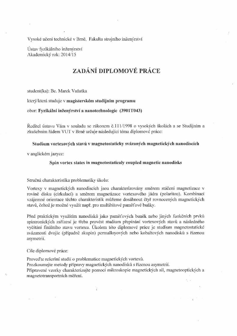

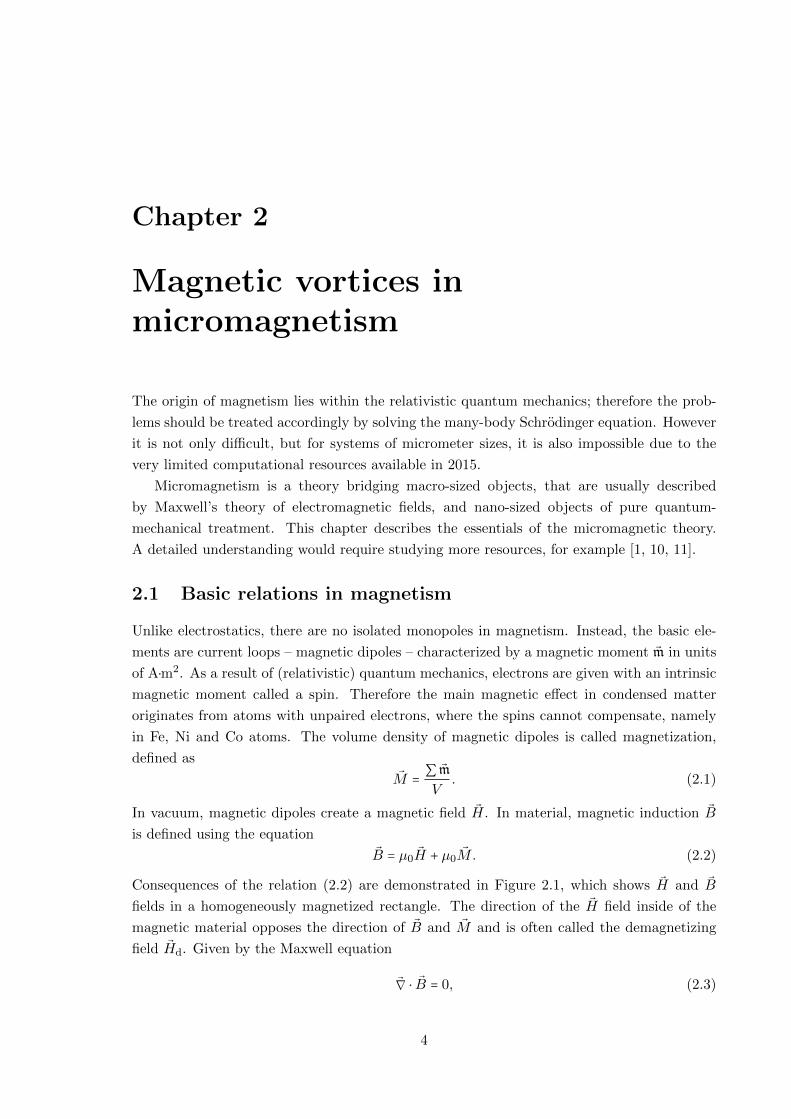
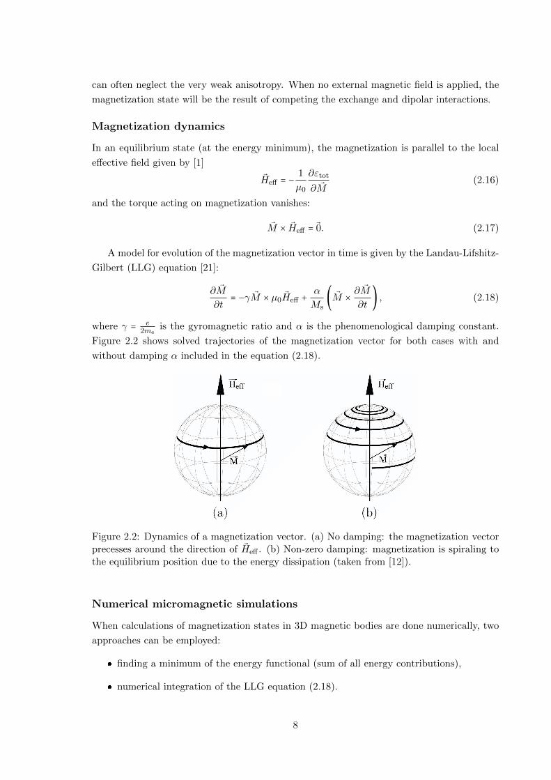
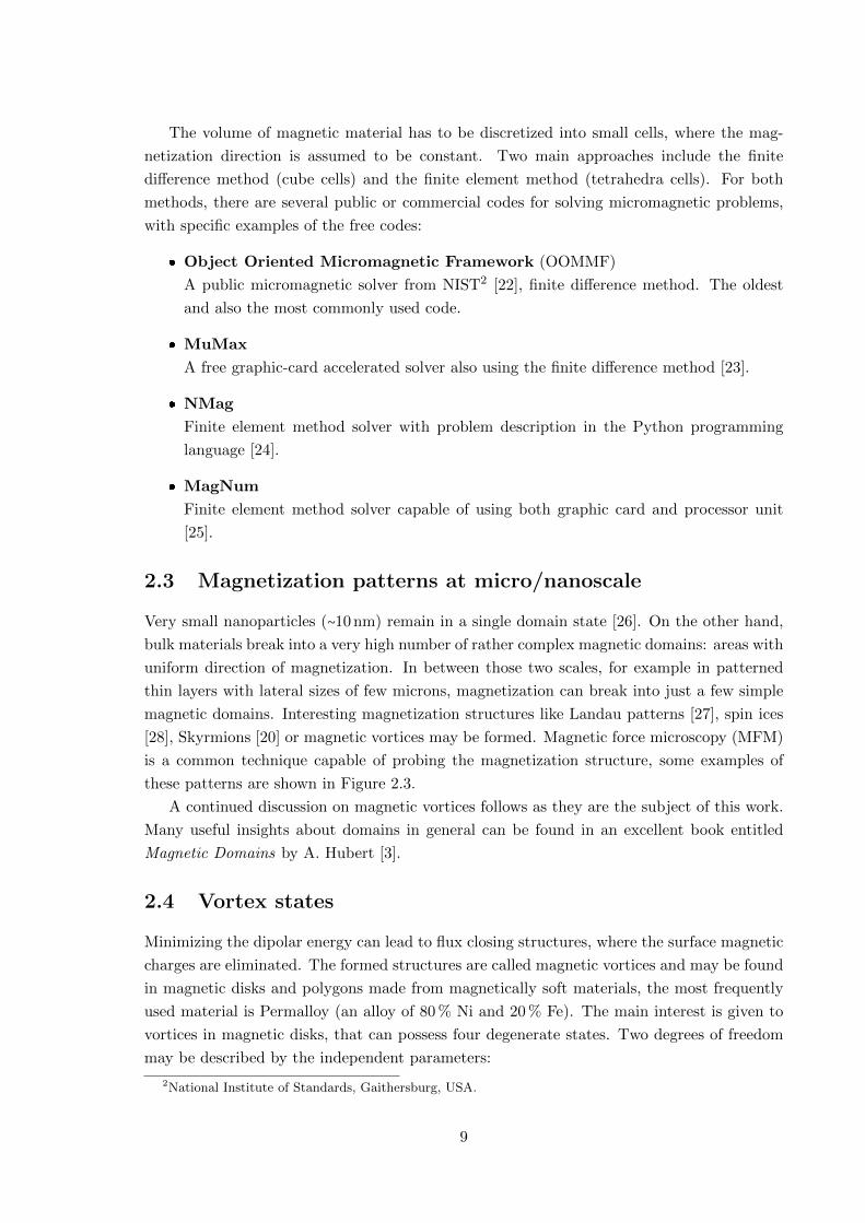
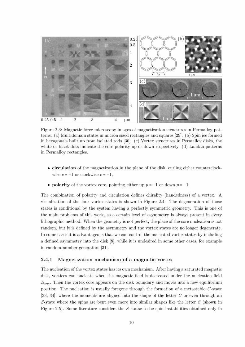
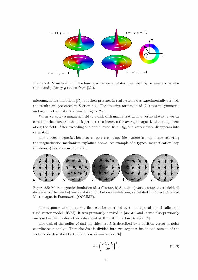
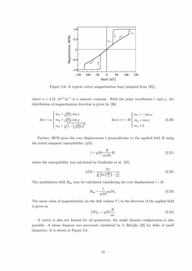
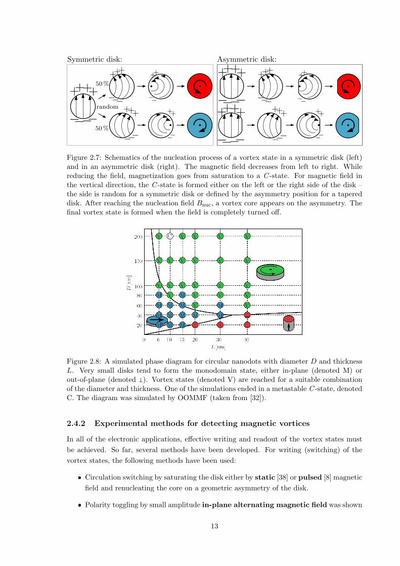
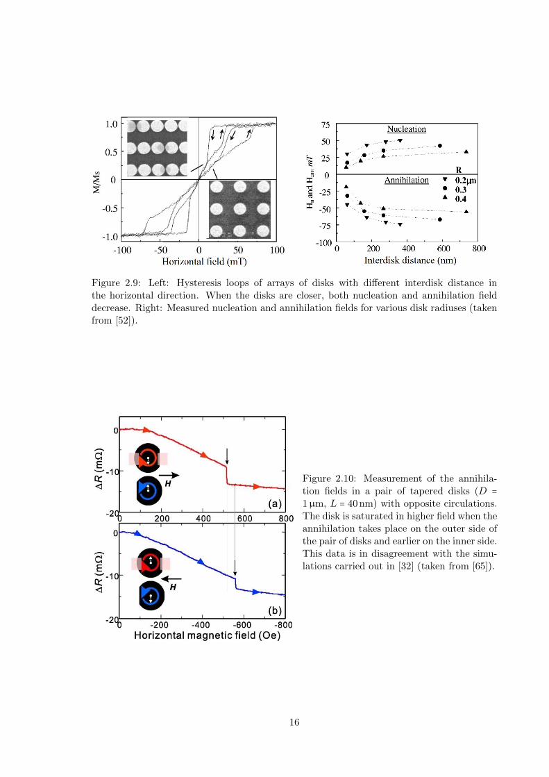
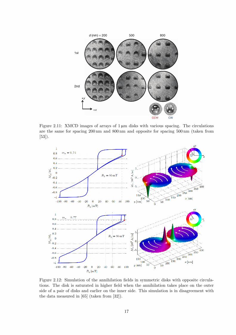
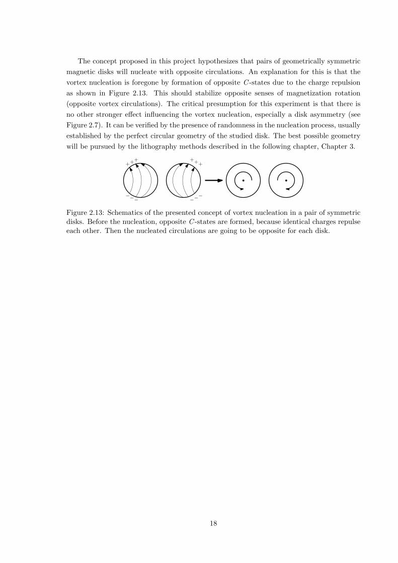
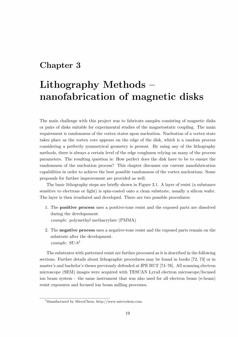
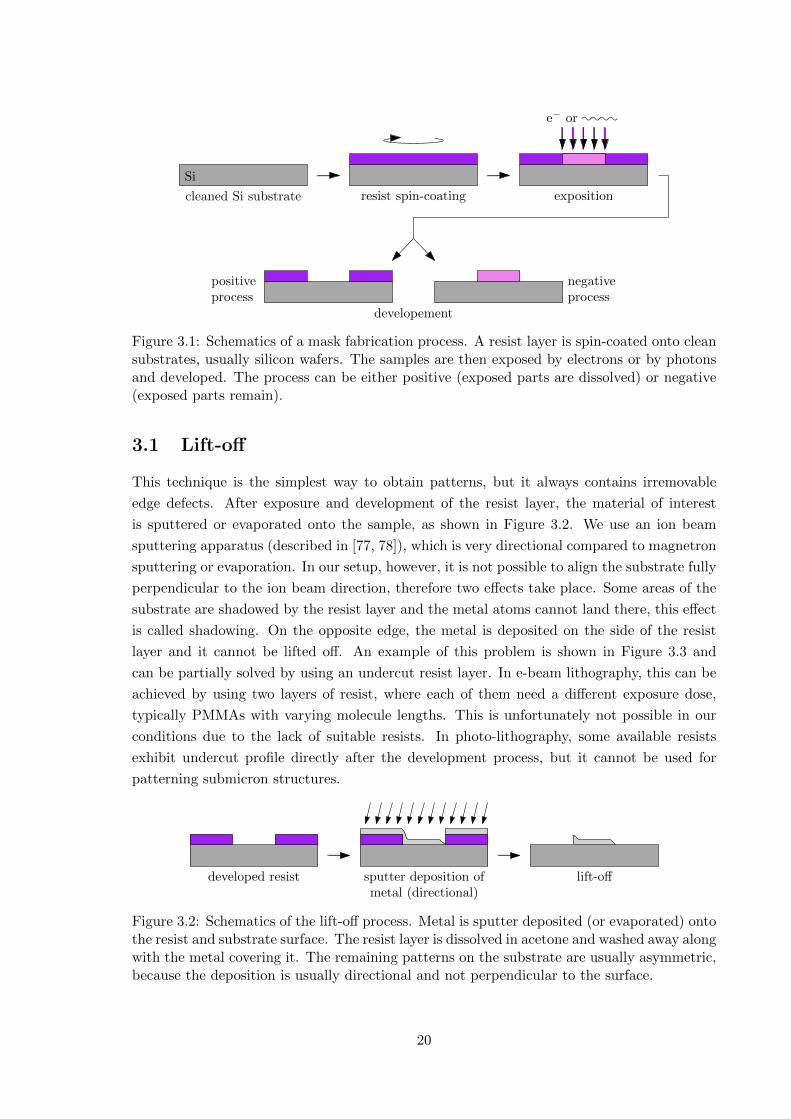
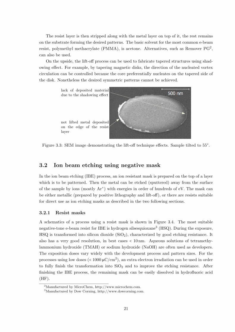
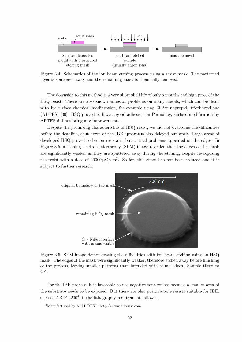
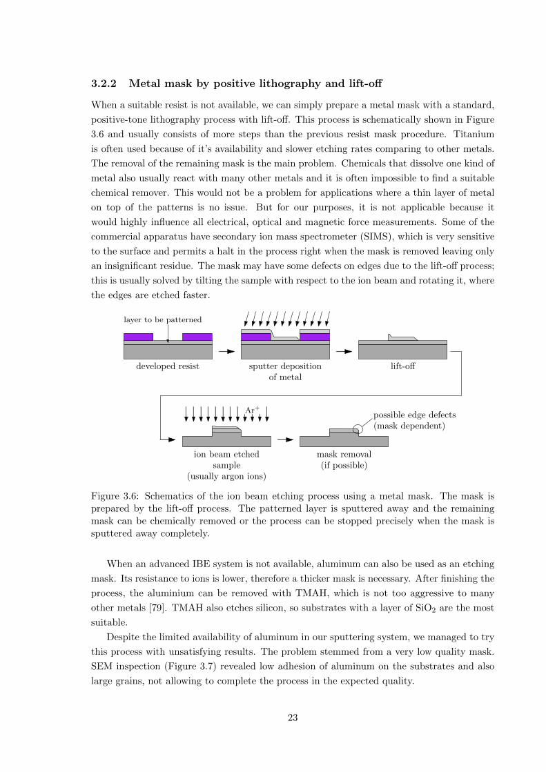
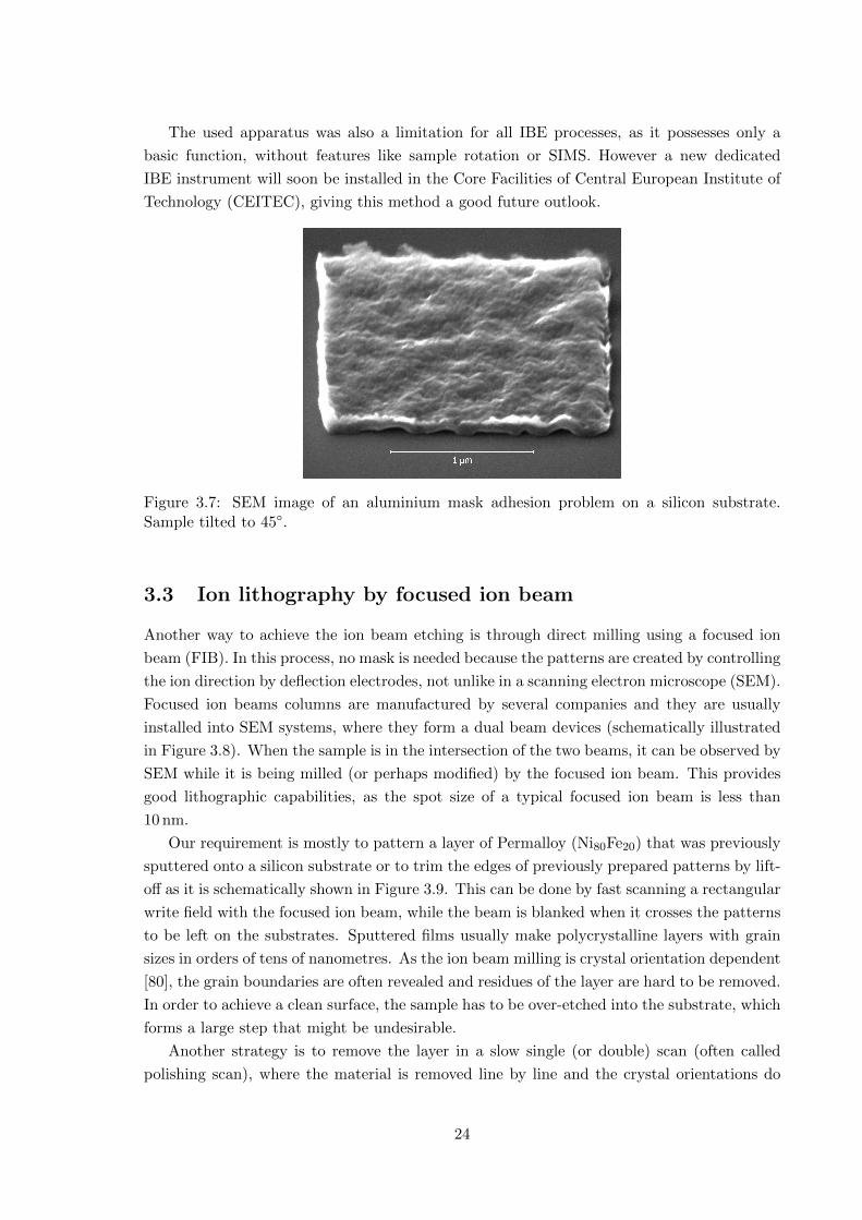
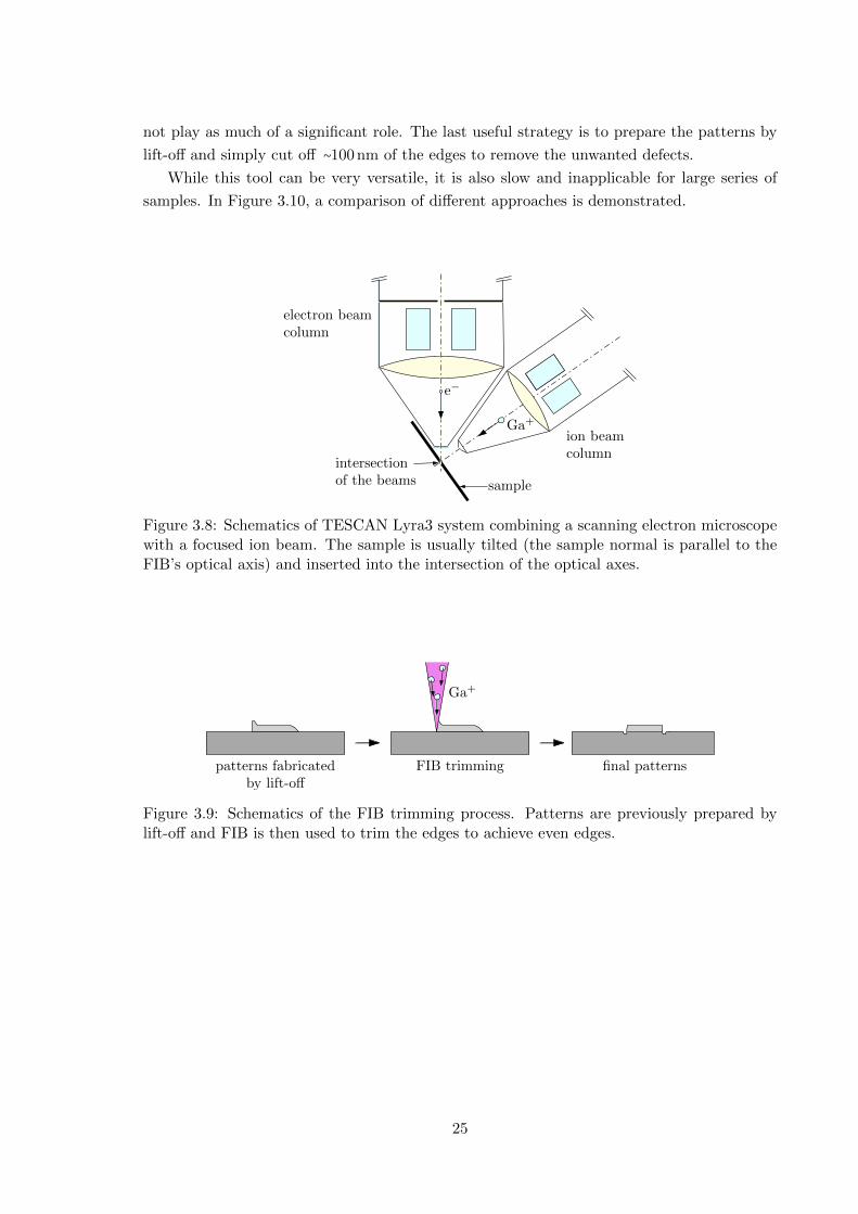
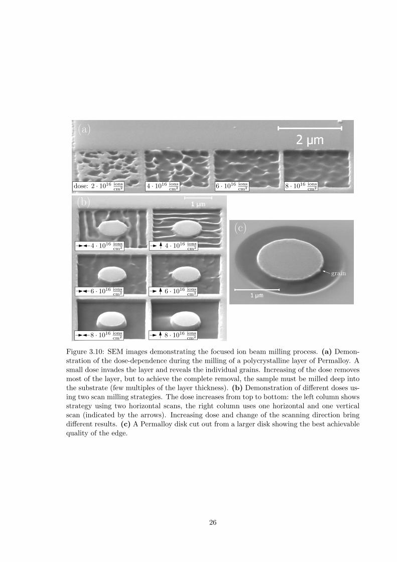
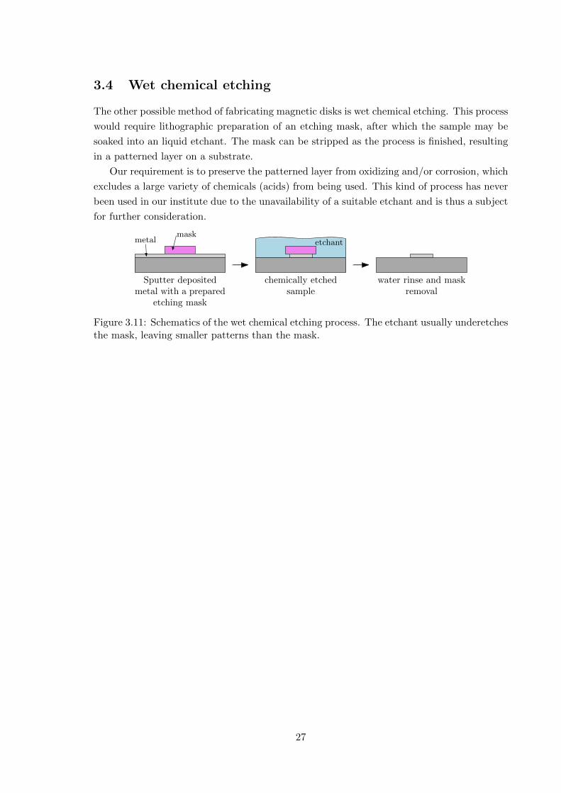
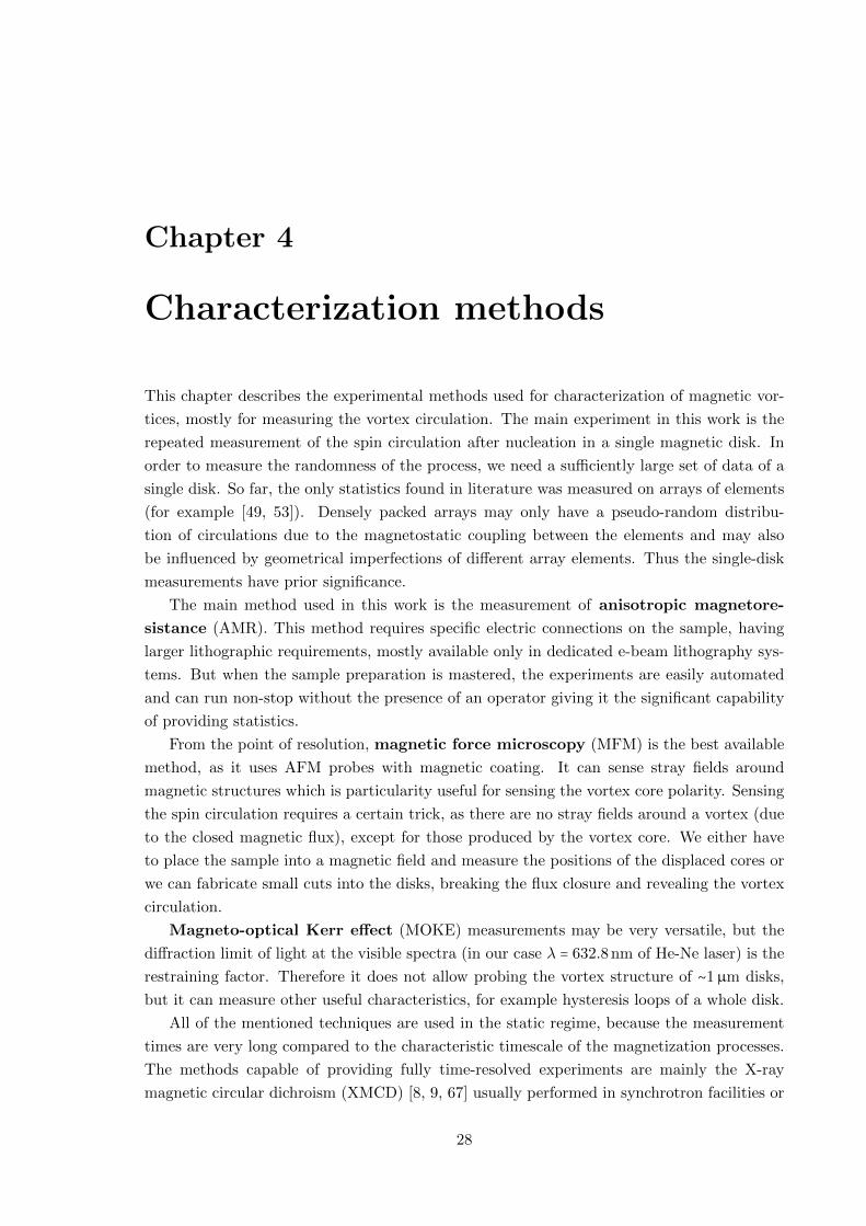
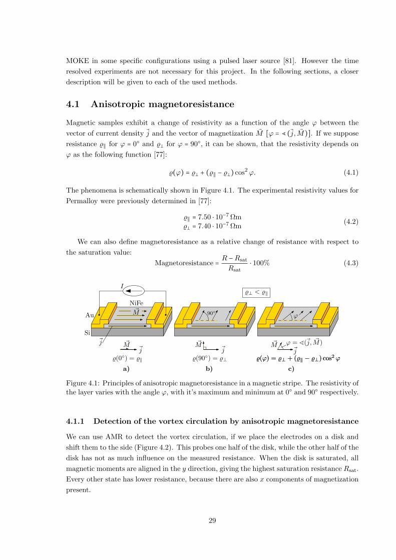
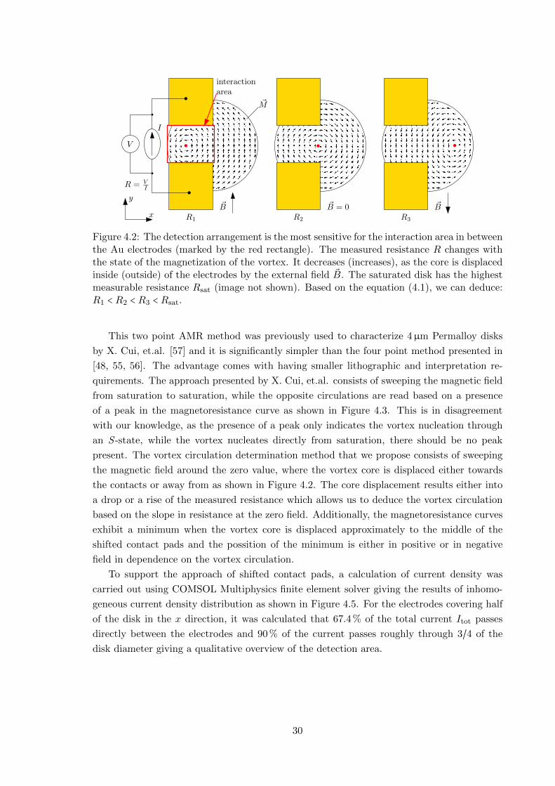
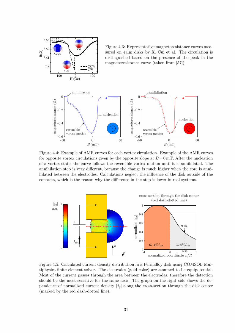
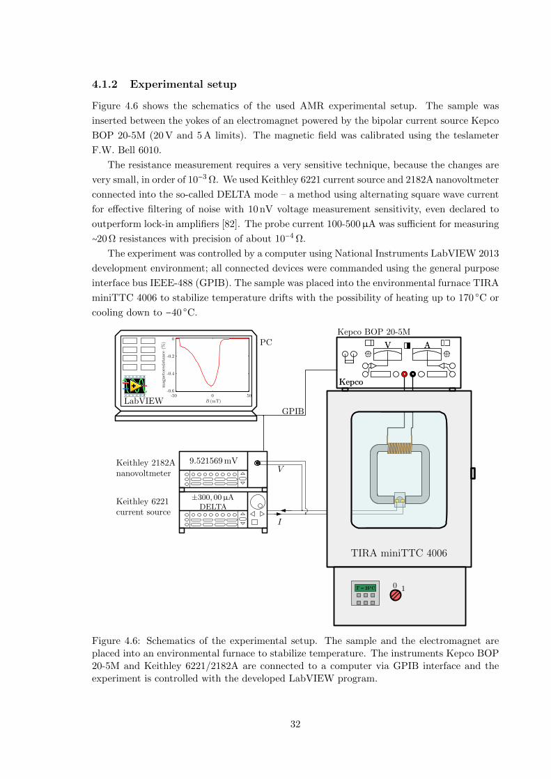
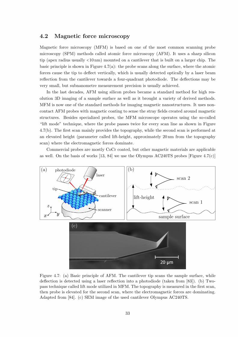
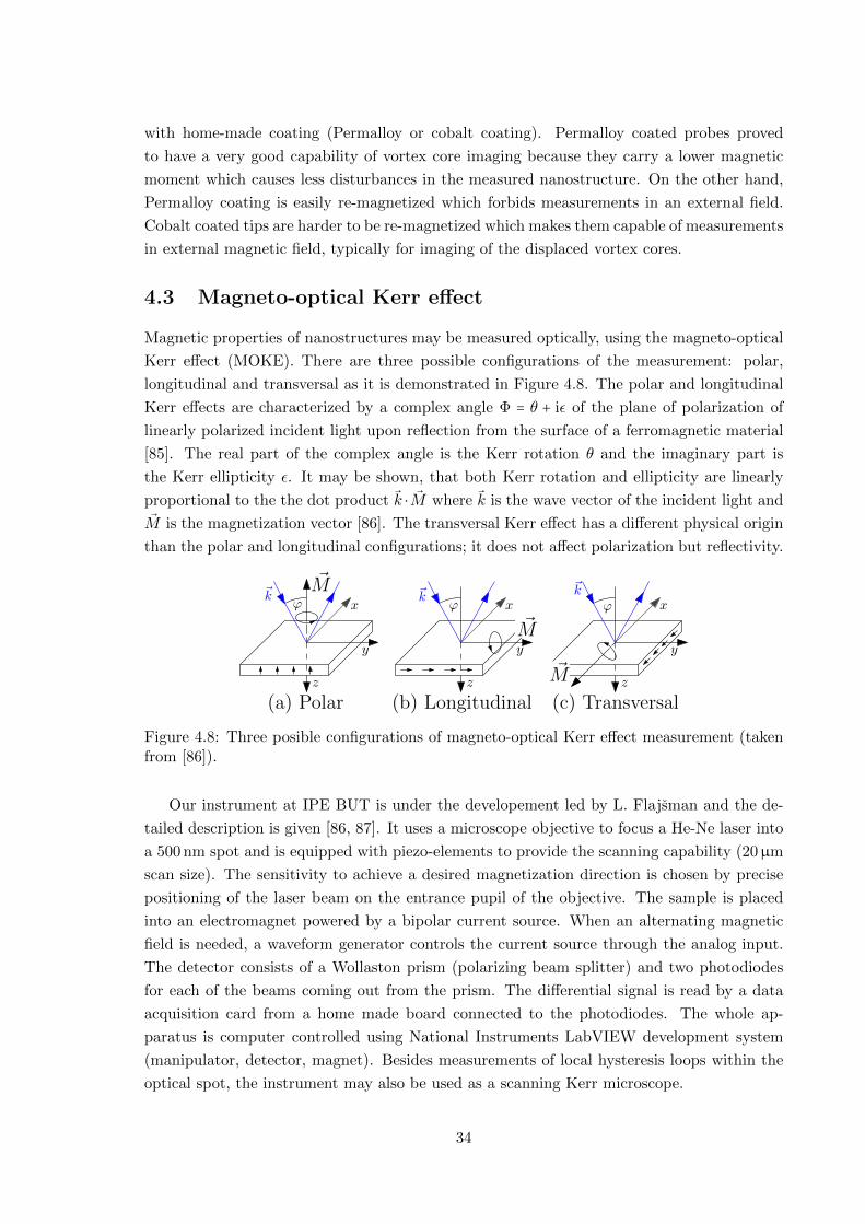
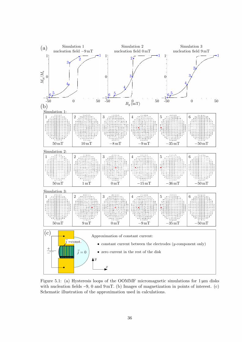
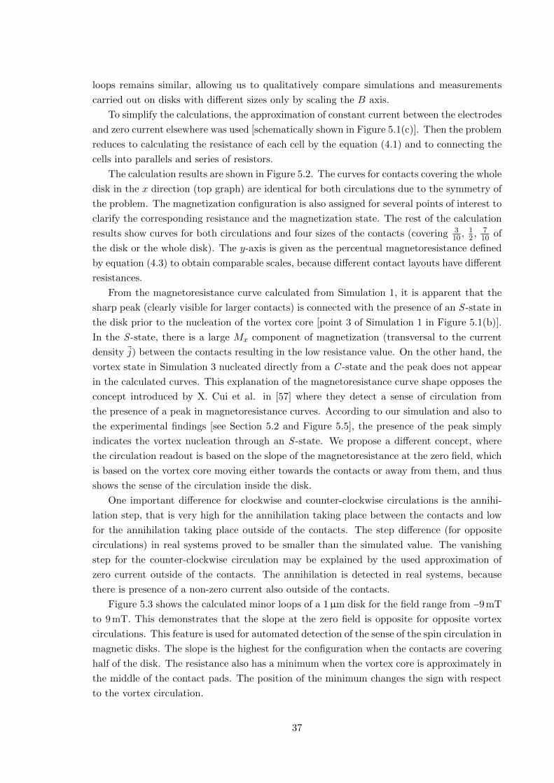
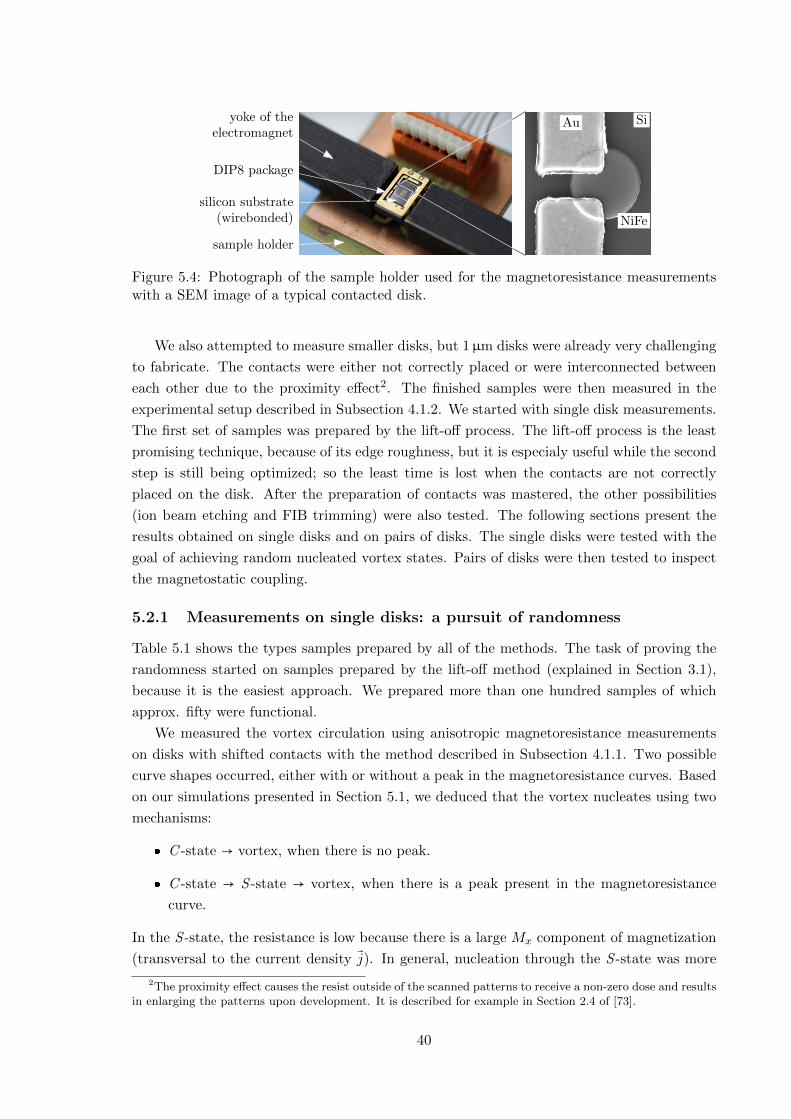
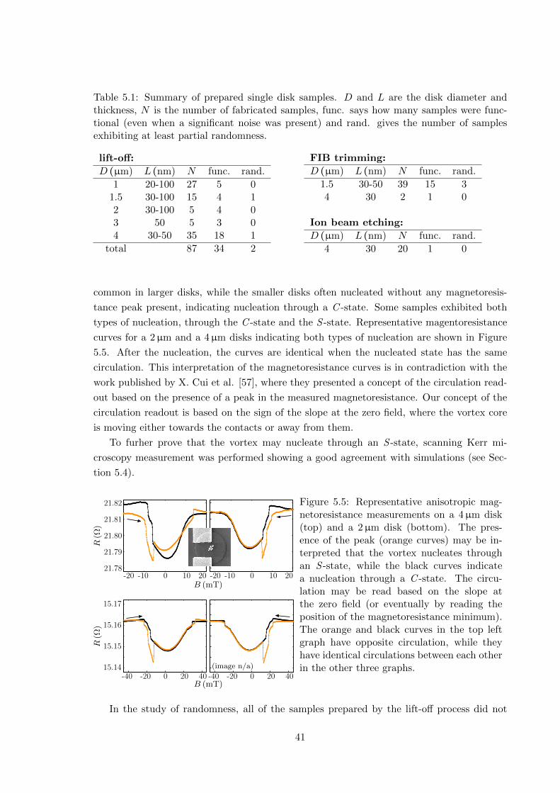
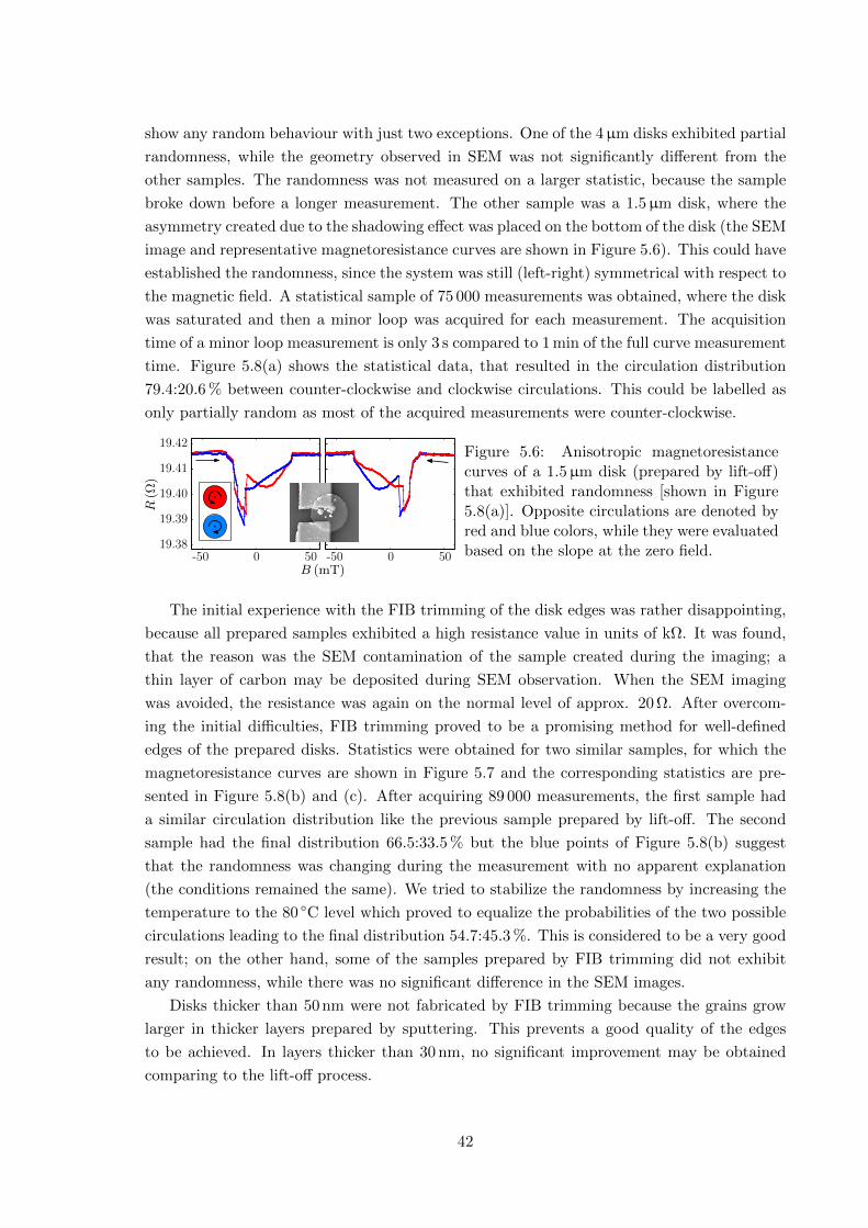
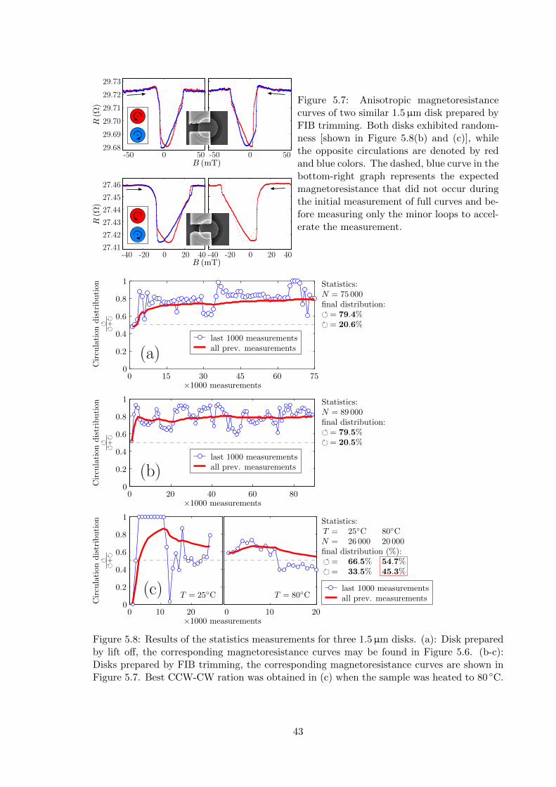
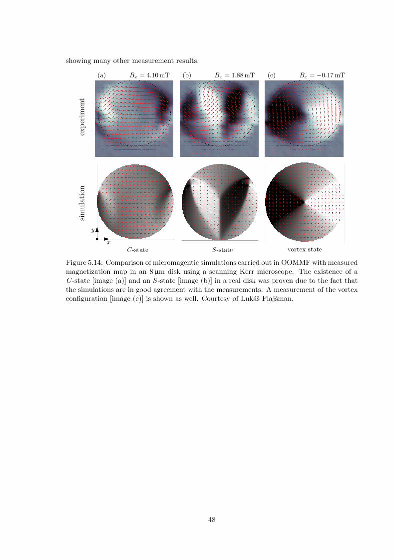


![VYSOKE U CEN I TECHNICKE V BRN E - core.ac.uk · Seznam odborné literatury: CHAFFEY, Dave; SMITH, PR. EMarketing eXcellence. 3. [s.l.] : Butterworth Heinemann, 2008. 508 s. ISBN](https://static.dokumenty.site/doc/80x56/5b5dba507f8b9a3a718ecd3f/vysoke-u-cen-i-technicke-v-brn-e-coreacuk-seznam-odborne-literatury-chaffey.jpg)


